How Far Apart Should the Traces Be?
The minimum space between conductors is determined by the PEAK VOLTAGE difference
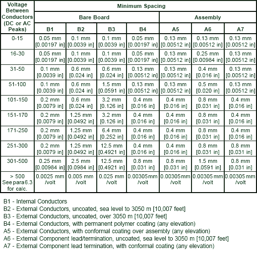
This is Table 6-1 of IPC-2221 (Generic Standard on Printed Board Design), which lists the minimum spacing between conductors for various conditions such as internal vs. external, coated vs. uncoated, high or low altitude, and traces vs. component leads
Keep in mind that these are MINIMUMS, and other guidelines or specifications may take precedence. For example, designs that must meet Underwriter's Laboratories (UL) approval will have greater spacing requirements. Other factors such as humidity and pollution may also affect performance, so it may be wise to maintain extra clearance if the design will allow it.
Two terms used in calculating appropriate distances between conductors are creepage and clearance, but a good explanation of these is beyond the scope of this tutorial (and beyond my ability!). A simple introduction to these concepts can be found HERE, or at the "Compliance Engineering" website.
An online Creepage/Clearance calculator based on IEC 60950 requirements can be found at http://creepage.com


How Wide Should the Traces Be?
Appropriate Trace Width is determined by the CURRENT requirement and acceptable TEMPERATURE RISE
DETERMINING CIRCUIT BOARD
CURRENT CARRYING CAPABILITY
Determining appropriate trace sizes for current requirements is an important aspect of circuit board development. Since copper is not a perfect conductor, it presents a certain amount of impedance to current flowing through it, and some of the energy is lost in the form of heat. For many applications it is necessary to predict the temperature rise caused by this loss, which has been accomplished traditionally by using a chart created over fifty years ago by the National Bureau of Standards (currently Figure 6-4 in the IPC-2221 Design Guideline), or by using one of several calculators based upon it. The chart shows the relationship between current, conductor temperature rise and conductor cross-sectional area. If any two of these are known, the third can be approximated.
About ten years ago, Mike Jouppi of Lockheed Martin began performing experiments to examine the accuracy of this chart, because the predicted temperature obtained from it did not correspond to the data he was measuring on an actual product. From this new data he developed several new charts, which have been verified by a parallel study performed by the Naval Surface Warfare Center, Crane Division.
The results of both studies were compiled into IPC-2152 as the "Standard for Determining Current Carrying Capacity in Printed Board Design", published in August 2009. From the data presented in this new document, a method can be established to predict the temperature rise of a circuit board trace more accurately, taking into account the effect of several variables such as board thickness and material, internal vs. external traces, still air environments vs. vacuum, and proximity to heat-sinking planes. Estimations using this new data can be far more reliable than was previously possible, without the use of more sophisticated thermal analysis tools.
THE HISTORICAL CHART
IPC-2152 contains over ninety new charts in addition to the historical chart we have been using, but before exploring the new data, a few aspects of the historical chart should be understood. When the first chart was created in the 1950's, there were no multilayer boards and all of the data was taken from surface traces. The internal chart was added many years later. No one is sure where the internal chart came from, but it is thought that when multi-layer board constructions became practical, the external values were merely doubled to get values for internal traces. This has since proven to be inaccurate. The thermal conductivity of FR4 is better than air, so in a still-air environment the internal traces actually run cooler than external. The internal values are so conservative, however, that designers haven't experienced problems using them except for the large amount of board real-estate needed to implement the recommendations.
An interesting result of the new study was the fact that, although the values for internal traces were not scientific, by coincidence they very closely approximate the behavior of traces in free air. The new data also showed that the external trace chart was only safe for boards greater than 3x3in and with planes, so it was decided to remove the historical chart for external traces from IPC-2152. Recommendations for external traces can be easily obtained with the new charts and adjusted for the proximity to heat-sinking planes.
Since the internal chart values approximate the temperature rise of a trace in free air (which can be considered a worst-case scenario), it was decided to use it for the most conservative chart. Values obtained from this chart are very safe and will work in any circumstance except vacuum, regardless of other variables.
Conservative Chart
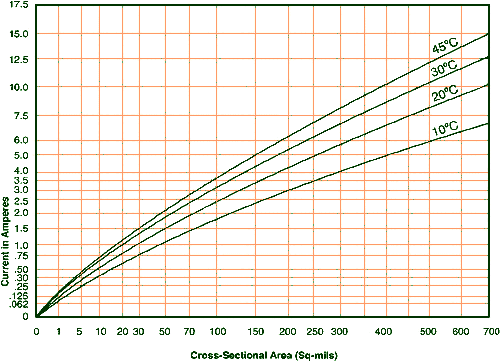
For example, let's say a trace in a very thin flexible dielectric must carry 4 amps continuously, and you want to limit the temperature rise to 10°C over ambient. To use the conservative chart, follow the 4.0 amp current line across until it intercepts the 10°C temperature curve. Follow that intersection down to find the recommended cross sectional area of 300 square mils. This cross-sectional area can be refined further by modifying it with known design constraints. These adjustments are described in the section "Modifying the Chart Value".
After the recommended cross sectional area is determined, it can then be converted to appropriate trace widths (based on the copper thickness used in the design) by using a chart presented later in this article.
NEW CHARTS
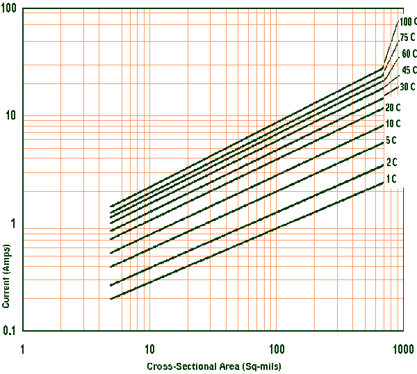
The chart in the preceding paragraph provides very safe estimates for most applications. For a more precise estimate based on specific design constraints, new charts have been developed. Since circuit board development often depends on common laminate materials with common copper weights, separate sets of charts are provided based on .070 inch polyimide material with 3oz, 2oz, 1oz and half ounce copper in still air. For each of these there is a primary logarithmic chart, like the one shown below. This is the baseline chart for 3oz copper, which is the universal chart used in IPC-2152 Figure 5-2, recommended for both internal and external traces:
Universal Chart
Since logarithmic charts are difficult to read, each of these primary charts is followed by three additional charts that show temperature curves at successively finer resolution. This has been duplicated by another complete set of charts for vacuum environments, and all of these are duplicated again to provide versions for inch and metric units. There are also charts in the appendix for internal vs. external traces.
(For the purposes of this tutorial, we will look up a starting value from the universal chart and then modify it for our particular design constraints. If you have the extra charts in IPC-2152, you can select a chart more specific to your application, and skip the corresponding modification outlined below.)
OBTAINING THE APPROPRIATE CHART VALUE
The first step in estimating appropriate trace widths is determining the acceptable temperature rise. This is an important point, because most circuit board designers are familiar with the term "ambient temperature", which is a simple term to describe the environment in which the electronic assembly operates. For our application the term ambient temperature can be misleading, because the temperature rise of the trace is going to be higher than all of the contributing factors combined. This is not just the ambient temperature, it is the ambient temperature plus all of the other heat sources of nearby components and traces. For this reason the new standard has preferred the term "local board temperature" to ambient temperature. The local board temperature can be significantly higher than the surrounding environment, and the temperature rise of a single trace is added on top of that. For example, your product may be required to operate in an ambient temperature of 125°C, and the area of the trace you are evaluating may have power devices and other high current traces in close proximity. The local temperature may already be approaching the maximum continuous operating temperature of the board material itself, and it you may need to define a lower temperature rise for the single trace. (Parallel traces are a critical factor that should not be ignored. The added temperature from surrounding traces can have a significant effect on the local board temperature, and should be considered in every evaluation. IPC-2152 Appendix A.3.3 discusses this in detail)
In general, traces operating at high temperature wastes power and adds thermal stress that may lead to early failure, so a low temperature rise should be a design goal whenever possible.
Once you have settled on an acceptable temperature rise for the trace being evaluated, it is a simple matter to find the cross sectional area required for the current requirement, using either the conservative chart or the new universal one (use the new one only if your board is greater than 3x3in!).
MODIFYING THE CHART VALUE
If the conservative chart was used to obtain the starting chart value (CV), it can be used AS IS without the need for any additional analysis. If the new universal chart was used to obtain the CV, keep in mind that it is based on a board that was constructed with 3oz copper on polyimide material .070 inches thick. To get a more accurate estimate, you can perform modifications to the CV based several possible conditions before converting it to a recommended trace width . The easiest way to do this is to format the known data for each parameter as a percentage change, and then multiply it with the CV to derive the recommended cross-sectional area. This Modified Value can then be used to determine the appropriate trace width.
For each specific design parameter,
estimate the multiplier and use it to adjust the CV:
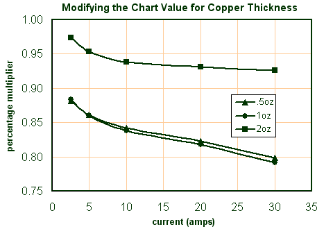
Copper Thickness Multiplier
If the universal chart above was used to obtain the CV, and you are not using 3oz copper, you can take advantage of the fact that for the same cross-sectional area, thinner copper has more surface area and is therefore better at dissipating heat. Thicker copper will have thinner trace width for the same cross sectional area, less surface area, and will operate at a higher temperature.
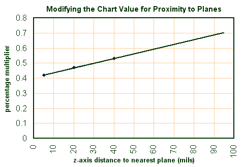
Plane Multiplier
Since the proximity to heat-sinking planes has such a drastic impact on the temperature, the presence of planes will cause the most significant adjustment to the CV. For boards with a 1oz plane that is at least a 3x3in. area (directly UNDER the trace being evaluated!), use the following chart to determine the modifier:
For 2oz planes, reduce the Chart Value an additional 4% (.96 multiplier)
For planes greater than 5x5in, reduce the Chart Value an additional 4% (.96)
Board Material Multiplier
The polyimide material that was used in the study has a thermal conductivity of .0138 and FR4 is slightly worse at .0124, which makes a difference of about 2% in the CV. Materials with different thermal properties may influence the recommendation.
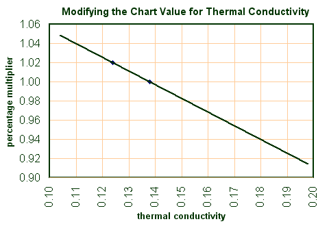
For FR4 boards, increase the Chart Value by 2% (1.02 multiplier)
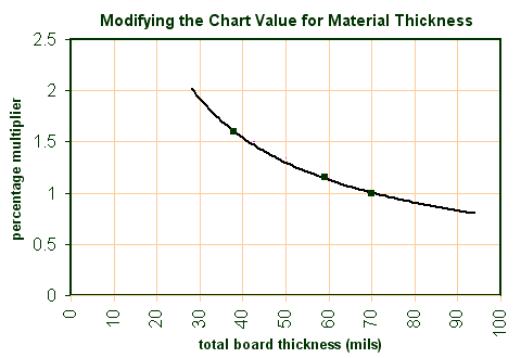
Board Thickness Multiplier
The new charts were constructed using data from boards that were .070 inches thick. Thinner boards will be hotter, and thicker boards will be cooler. (IPC-2152 A.4.2)
Altitude Modifier
This one may be refined further in the future, but knowing that air is thinner at higher altitude, and traces run 35-55% hotter in a vacuum, either the conservative chart should be used or the CV should be increased for high altitude designs.
De-rating Modifier
Keep in mind that the charts have no de-rating applied to them, but many variables may affect the CV prediction and should be considered for marginal designs. For example, the planes modifier is based on the assumption that the trace sits over a solid plane, but in actual practice may be located near a board edge or over a plane that has clearances in it for through-holes or plane splits, which will be less effective in dissipating heat. Process variations that affect the trace geometry may also influence the results (in the form of voids, nicks, over-etching, final plated conductor thickness, etc.). These variations all have acceptable tolerances in the finished product, but may affect the estimated temperature rise. It is advised that some amount of standard de- rating be applied to the CV, but a full examination of this modifier is beyond the scope of this article.
Consider increasing the Chart Value for a safety margin
Environmental Modifier
The new data describes traces in still air (which assumes some amount of natural convection), so these recommendations should be valid even for applications inside a sealed enclosure. But for many other applications, air flow will be present, and this additional heat transfer may allow a reduction in cross sectional area. This is a complicated subject, and recommendations related to air flow are beyond the scope of this article. Some thermal analysis may be needed if the designer needs to use thinner traces than what the available data suggests.
OBTAINING THE FINAL TRACE WIDTH
At this point you have selected a value from one of the charts and modified it for your specific design parameters.
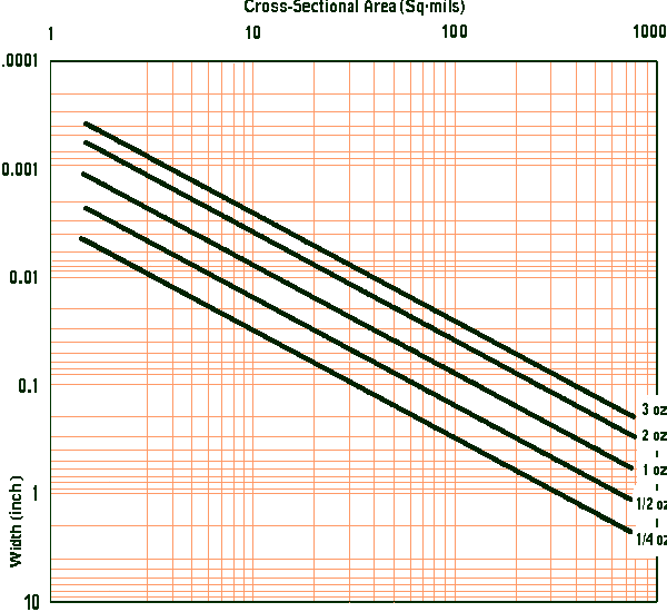
The final step is converting the resulting cross sectional area to the final trace width, based on the thickness of copper you will be using in the board construction. This step should not be confused with the modification based on copper thickness to account for varying surface area. The chart below is a direct correlation between cross sectional area and (copper thickness x trace width):
FOR EXAMPLE:
Let's assume we are designing a 4-layer circuit board using FR4 material that will be 3x5in by .063 inches thick, and the two internal layers are power and ground planes that are 20 mils away from the surface layers. We need an external trace that can accommodate 10amps continuously, and we want to limit the temperature rise to 20°C above the local board temperature.
We could use the Conservative Chart to get a 680 sq.mil cross sectional area, and use the final conversion chart for 1oz copper to get:
Trace Width = 530mils
That's the easy answer, and if the board design allows, it can be used AS IS.
Since we have good information about our design, and the board is larger than the 3x3, we can use the Universal Chart instead of the Conservative Chart. Following the 10amp line across to the 20°C temperature curve, we see that it intersects with the line for a starting value of about 520 sq.mil cross sectional area.
CV=520
Next, we can modify based on the fact that we are using 1oz copper:
multiplier = 0.84, (520*0.84) CV=436
(we ignore the modifier for 2oz planes and also the one for large planes)
Since we have a 3" x 5" 1oz plane 20mils away, using the Planes Chart:
multiplier = 0.47, (436*0.47) CV=205
Our board thickness of 0.062 is less than .070, using Thickness Chart:
multiplier = 1.08, (205*1.08) CV=220
We are using FR4 instead of Polyimide, so using Material Chart:
multiplier = 1.02, (217*1.02) CV=224
And as a judgment call, we are going to add 5% for de-rating:
multiplier = 1.05, (221*1.05) CV=235
Using the final chart to convert 235 sq.mils to a 1oz Trace Width, we get
180 mil Trace Width
The Historical Chart would have recommended a 250 mil Trace Width for a 10amp 1oz external trace, which illustrates how this new data can be used to "push the envelope". In many cases the design can be accomplished with less board space, using appropriate parameters to derive the estimate.
FOR EVEN MORE ACCURATE RESULTS...
This tutorial has been only a brief introduction to sizing traces for current requirements.
The IPC-2152 publication, "Standard for Determining Current Carrying Capability in Printed Board Design" contains more verbose explanations, nearly a hundred more charts (including a complete set in metric), and a wealth of supplementary material in the appendix such as the evaluation of parallel conductors, etched coils, vias and microvias, power and voltage drop analysis, HDI and high speed skin depth, and data for vacuum environments.
(Thanks to Mike Jouppi for his persistence, and to Borko Bozickovic for helping with data)