It will be easier to understand bare board materials if you have a general idea of how a circuit board is fabricated. There is a lot to learn about circuit board manufacturing, but for now it will be enough to understand only a few basic steps.
Most circuit boards are constructed with layers of conductive copper separated by insulating layers of flame-retardent fiberglass material, which is composed of woven glass cloth impregnated with epoxy resin. The unwanted copper on the conductive layers is etched away, leaving only the desired circuitry, and holes are drilled and plated to connect layers together. The board is then coated with soldermask (usually green) to cover everything except the solderable surfaces, fiducials and test points. A graphic/text silkscreen legend may be applied using a contrasting color (usually white). The copper that is left exposed is then coated with a protective finish to prevent corrosion, or tarnishing.
This is a brief summary of the process used to fabricate most multi-layer circuit boards:
BARE-BOARD FABRICATION
IN 10 EASY STEPS
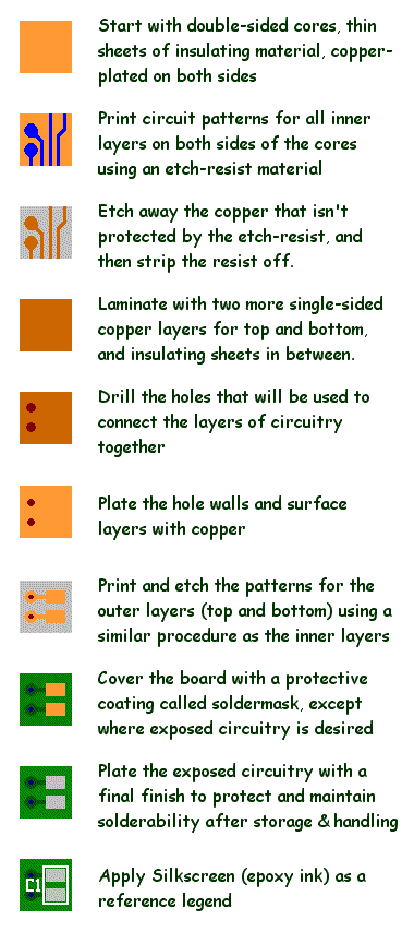
That short list is enough about fabrication to convey the idea that to make a circuit board, you will specify several different types of material; laminates for the board stack-up (insulating material separating conductive material), a mask material to protect most of the board surface, a final finish to protect the exposed solderable areas, and a material for the silkscreen ink.
To learn more about circuit board fabrication:
- Click [HERE] for a very good "Virtual Tour" of the board fabrication process with photographs of the equipment used in each step (contributed by a knowledgeable fan, THANKS!)
- Arrange a tour of a local board supplier, if one is available in your area. (It's good advice to get out of your cubicle and see the real world of electronics manufacturing at least once in your career. Don't be afraid to ask questions!)
- The Printed Circuits Handbook assembled and editied by Clyde Coombs is probably the most comprehensive description of circuit board manufacturing available (includes sections on related technologies, planning, materials, fabrication, assembly, test, quality and environmental concerns and covers both rigid and flexible board constructions).

Circuit Board Materials
Circuit boards are made with copper conductors separated by insulating materials which are typically resin systems with a reinforcement material to add strength and stability. The most prevalent materials are FR-4 Epoxy systems (which means Flame Retardent) reinforced with layers of woven glass cloth, but other resin systems are available like Polyimide (Kapton) or PTFE (Teflon), or with more exotic reinforcements like Kevlar or quartz. A variety of options have been developed to enhance specific desired properties (for example, better thermal performance or lower signal loss), but of course they are more expensive than common FR-4 materials.
An attempt has been made by the electronics industry (a committee of volunteeers organized by the IPC) to classify materials according to their properties and sort them into groups. This has been published as IPC-4101, the Specification for Base. Materials for Rigid and Multilayer Printed Boards, which continues to be expanded and revised as new materials become available. In IPC-4101, materials with similar properties are grouped by number, and each numbered data sheet is referred to in the industry as a "slash sheet". Most material data sheets will list the IPC slash sheet numbers that they conform to.
Laminate materials (also called "cores") are manufactured and sold in large sheets, typically around 36" x 48", and then cut into smaller fabrication panels by the bare board fabricator. They are fully cured and coated with a thin layer of copper on both sides. Pre-Preg materials (sometimes called "B-Stage"), are glass cloths pre-impregnated with resin, but are not fully cured. One or more pre-preg layers will be inserted between each core to complete the layer stackup, and it is these pre-pregs that melt in the lamination press, forming the adhesive that bonds the layers together.
Material Properties
The following characteristics will be more or less important depending on the particular application. They may have to be prioritized to find a balanced solution that meets the cost and performance targets of the product.
Coefficient of Thermal Expansion (CTE)
Most materials expand when their temperature rises, and contract when they cool. CTE is a way of expressing the amount of change in a material's volume during a temperature change, expressed as parts per million per degree centigrade (ppm/%deg;C). One way of classifying materials is by comparing their CTE. Epoxy resin has a CTE (35-45) that is higher than copper (17-18). This would be a mismatch during thermal cycling that could lead to early failures, but the fiberglass reinforcement material has a much lower CTE (5-6) that limits the expansion in the X-Y directions. This added glass brings the overall CTE of a laminate very close to that of copper. Nothing constrains the expansion in the Z-direction, however, so many designers use materials that are rated based on their z-axis CTE. For example, many designers specify materials that expand no more than 3% of their thickness (z-axis) over a temperature change from 50%deg;C to 260%deg;C
Tg - Glass Transition Temperature
As temperature changes, the expansion or contraction of a board material will exhibit a fairly linear rate of dimensional change, as shown in the figure below. At the glass transition temperature, the material changes from being in a hard and relatively brittle condition to being in a viscous or rubbery condition, and the rate of change will vary drastically.
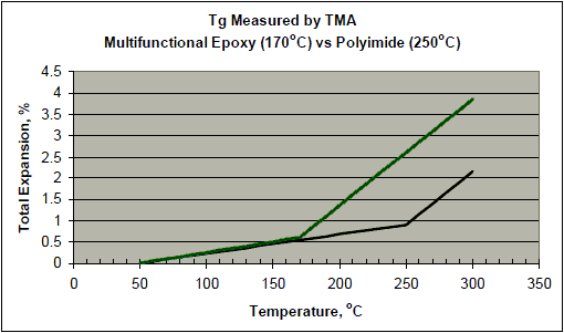
In the figure above, you can see that both materials behave very nearly the same at low temperatures, but the material with a lower glass transition temperature begins to change significantly more above 170°C. Materials with low Tg might be okay for applications that use eutectic solder (which melts at 183°C) but might not be acceptable for lead-free solders that require temperatures above 220°C.
Td - Decomposition Temperature
The temperature at which a base laminate material experiences an established percentage of weight loss using Thermogravimetric Analysis (TGA). Td is the temperature at which a material begins to degrade, most commonly specified as the temperature at which a material has lost 5% of its original weight due to decomposition. In the past, the glass transition temperature (Tg) has been used to classify materials by their thermal properties, but at the higher temperatures required for lead-free soldering (to meet RoHS requirements), Td has also proven to be a useful indicator of board material stability.
T266 T288 and T300
T260, T288 and T300 values represent the length of time that a clad laminate will survive a particular temperature (respectively 260°C, 288°C and 300°C) before it begins to delaminate or blister. These values are considered good indicators of the short term resistance of the material to the soldering process.
Dielectric Constant (Er)
The Dielectric constant (or "permittivity") determines the speed at which an electrical signal will travel in a dielectric material. Signal propagation speed is expressed relative to the speed of light in a vacuum, which is defined as having a dielectric constant of 1.00. Higher dielectric constants will result in slower signal propagation speeds. A common dielectric constant for FR4 materials would be in the range of 4.2 to 4.8, but for high-speed applications, materials have been developed that are in the range of 3.0 to 3.6. Other materials may be available with lower Er, but could be a significant cost adder to the product. For designs with Impedance Controlled signals, you will need to know the Dielectric Constant to calculate the appropriate trace widths to use.
Related to dielectric constant is Dissipation Factor, also known as Loss Tangent. This is a measure of the percentage of the total transmitted power that will be lost as power dissipates into the laminate material.
Specifying Laminates
If you send a design to be manufactured (to a "UL-approved" fabricator) with no materials specified at all, you should still receive an acceptable board for most applications. In other words, even without drawings or notes or instructions, and in the absence of any specific requirements, the fabricator still has the responsibility for using materials that provide proper interconnection between components and that provide adequate insulation between interconnecton points that should not be connected, or you shouldn't have to pay for the boards.
If you know in advance which fabricator will be manufacturing your boards and you have the ability to communicate with them, take the initiative to find out which materials they prefer to use. Don't be afraid to share your design criteria with them and discuss whether their default materials are adequate for your needs, or if you should specify something more robust. Regardless, don't hesitate to specify at least the general "slash sheet" number of material that will be adequate for your design needs.
Here is an example of a simple note to specify board material:
ALL MATERIAL MUST MEET OR EXCEED THE REQUIREMENTS OF IPC-4101/24
At the other extreme, here is one recommendation for a note specifying materials used in a RoHS-compatible high-reliability product:
BASE MATERIAL SHALL BE FLAME-RETARDANT RATED UL 94V-0 LAMINATE GLASS
FIBER EPOXY AND CONFORM TO TYPE L126 (GFG) ACCORDING TO IPC-4101/126.
BASE MATERIAL REQUIREMENTS: A MINIMUM GLASS TRANSITION TEMPERATURE OF
170 DEGREES C, AS TESTED ACCORDING TO IPC-TM-650, 2.4.24C; A MINIMUM
DECOMPOSITION TEMPERATURE, Td(5%) OF 340 DEGREES C, AS TESTED ACCORD-
ING TO IPC-TM-650, 2.4.24.6; A T-288 DELAMINATION TIME OF 10 MINUTES
MINIMUM, AS TESTED ACCORDING TO IPC-TM-650, 2.4.24.1C; MAXIMUM THICK-
NESS-DIRECTION THERMAL EXPANSION OF 3.0% FROM 50 TO 260 DEGREES C.
PREPREG MATERIAL SHALL CONFORM TO TYPE P126 (PGFG) ACCORDING TO IPC-
4101/126 AND BE SUBJECT TO THE SAME REQUIREMENTS AS THE BASE MATERIAL.
There may also be reasons for specifying laminate thickness to control the distance between individual layers. Examples could be:
- specifying a minimum distance between layers to maintain a voltage clearance requirement
- specifying a maximum separation between power and ground planes to maintain capacitance for decoupling
- specifying a desired distance between layers to achieve impedance targets.
For reasons such as these, you should also provide a desired layer stack-up with any requirements noted, and make sure to include the overall finished board thickness.
Keep in mind that this is only the briefest overview possible to introduce the concept of board materials. I have to focus on the most common type of board construction, but you should understand that there many options available for a wide variety of applications including flexible circuitry, metal-core constructions for high-temperature, exotic materials for high-speed signal propagation, special materials for High-Density Interconnect (HDI), materials for buried capacitance, etc. Each of these materials will have its own set of unique properties that contribute to the desired performance.
To learn more about board materials, see "Everything You Ever Wanted to Know About Laminates... But Were Afraid to Ask", by Chet Guiles at Arlon.
Specifying Copper
Copper is the conductive material that forms the connections between components, and serves as power and ground planes if the product is designed to take advantage of them. Copper also distributes heat, and becomes part of the mechanical strength for component attachment to the board.
Electro-Deposited (ED) copper foil is the standard copper used in the laminate industry. ED foil is deposited from solution onto a moving titanium or steel drum, from which it is subsequently stripped. The grain structure formed by this process forms the dendritic "tooth" of the copper foil on the bath side of the copper. The drum side takes the smooth texture of the polished drum surface onto which it is plated.
Rolled copper is made by running a copper strip through successively smaller and smaller gaps in a rolling mill until it reaches the desired thickness. Rolled copper is smoother and can be made very flexible by annealing (The acronym "RA" means "Rolled Annealed"). Much of the RA foil in the laminate industry is used in flexible circuitry, typically bonded to a polyimide film with an acrylic adhesive, used in applications where ductility is essential.
As a circuit board designer, the primary attribute of the copper in a board will be its thickness. Copper thickness is often specified in ounces; where one ounce copper would be the thickness resulting from taking one ounce of copper and spreading it evenly over a one square foot surface. Referring to copper thickness in ounces is a tradition dating back to when many roofs were covered with copper, and the tradesmen specified copper in this way. Although you need to know what people are talking about if they use phrases like "half-ounce copper" or "two ounce copper", it would probably be better for the circuit board industry to move towards specifying actual copper thickness, either in inch or metric units.
Here is a chart showing the dimensions of the most common copper thicknesses:
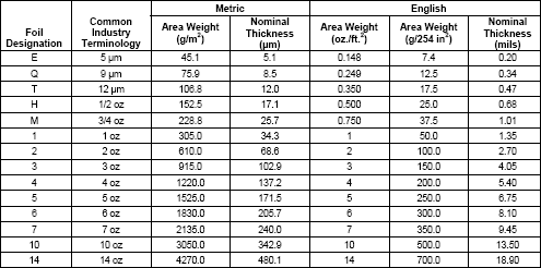
Using thinner copper makes it easier to control trace widths, but thicker copper can carry more current without as much heat. You may have to evaluate the current-carrying requirements of your design before selecting your material, but the most common copper weights range from half ounce to two ounce. A detailed tutorial on the relationship between trace geometry, current, and temperature rise (including a free spreadsheet-based calculator) can be found in the section called Trace&Space
If you look at a cross-section of copper clad material, you will notice that the outside surface is relatively smooth, but the side bonded to the insulating material has more "tooth". In other words, the bonded surface is more rough than the smooth exposed surface.
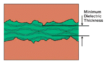
There are two things you should be aware of regarding the copper tooth:
- When measuring the dielectric thickness (the amount of insulating material), the distance is measured from peak to peak
- The skin effect of high-speed signal propagation may be affected by the copper tooth, and there are "low-profile" materials available to reduce this effect (materials with smoother copper, i.e. less tooth)
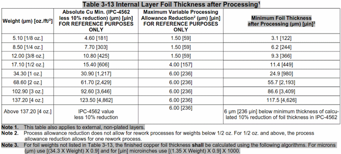
Finally, you should understand the fact that copper is specified with a theoretically exact thickness, but the actual thickness in any particular board construction can vary with accepted tolerances and as the result of certain processing steps in bare board fabrication.
Here is the allowance per IPC-6012 (Table 3-13) for FINAL INTERNAL COPPER THICKNESS :
Specifying Solder Mask
Solder Mask is the protective coating applied to the surface of most circuit boards, usually leaving only the solderable areas exposed. It is typically GREEN, although other colors are available. Requirements for solder mask are defined in IPC-SM-840 Qualification and Performance Specification of Permanent Solder Mask and Flexible Cover Materials. There are different categories of requirements based on the intended application, described as:
T - Telecommunication
This includes computers, telecommunication equipment, sophisticated business machines, instruments, and certain non-critical military applications. Solder mask and cover material on printed boards in this class is suitable for high performance commercial and
industrial products in which extended performance life is required but for which interrupted service is not life threatening.
H - High Reliability/Military
This includes equipment where continued performance is critical, equipment down-time cannot be tolerated and/or the equipment is a life support item. Solder mask and cover material on printed boards of this class is suitable for applications where high levels of assurance are required and uninterrupted service is essential.
FT - Flexible Printed Board Applications (Telecommunications)
This applies to cover materials for flexible printed board applications used in Telecommunications applications.
FH - Flexible Printed Board Applications (High Reliability/Military)
This applies to cover materials for flexible printed board applications used in High Reliability/Military Applications
The Flexible Cover Materials were added to revision "E" of the document. Requirements for solder mask materials correspond to the three "classes" of bare boards:
- Class 1 circuit boards have no requirement for solder mask,
- Class 2 circuit boards correspond to Class T/FT (Telecommunications) mask requirements
- Class 3 circuit boards correspond to Class H/FH (Military/high reliability) mask requirements
Solder Mask requirements specify parameters such as flammability, hardness, adhesion, shelf life, and resistance to soldering, moisture, biological growth, and to chemicals such as solvents, fluxes, and cleaning agents.
If conformance to IPC-6012 is specified on a fabrication drawing or in a procurement document, Solder Mask is automatically covered by IPC-6012 section 3.7 which states:
"When solder mask is required on printed boards, it shall meet the qualification/conformance requirements of IPC-SM-840. If a solder mask performance class is not specified for Class 1 or 2, IPC-SM-840 Class T shall be used. For Class 3, IPC-SM-840 Class H shall be used."
Regardless, designers quite often specify the mask in a separate note on the drawing. Here is an example:
SOLDERMASK OVER BARE COPPER PER IPC-SM-840 CLASS T, COLOR GREEN,
MATTE OR SATIN FINISH. NO MASK ALLOWED IN HOLES, ON FIDUCIALS OR
ON SOLDERABLE SURFACES. RESIZING FOR MINIMAL LAND TO MASK CLEAR-
ANCE IS ALLOWED.
One other consideration I've heard people discuss is the preference for MATTE or SATIN finish over GLOSS or SEMI-GLOSS. Some don't like the glare for manual processes and inspection, others say it reduces solder beading. You may want to ask your manufacturing partners what they prefer.
Specifying Final Finish
In the same way that a shiny new copper coin quickly begins to tarnish (turning a dull brown color), exposed copper on a circuit board quickly begins to oxidize. This does not affect the performance or conductivity of the copper itself, but it unless the copper is protected from oxidation it becomes very difficult to solder. To preserve the solderability of a circuit board, a FINAL FINISH will be applied to the exposed copper to protect it.
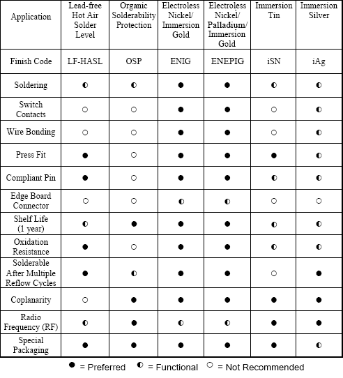
Hot-Air Solder Level (HASL)
Circuit boards were traditionally coated with solder itself, by dipping the entire board into molten solder and then blowing off the excess with hot air. HASL boards prove the solderability of the board in advance (problems with pad wetting are obvious with simple visual inspection before the assembly process begins), have a long shelf life and are easy to solder components to, for "Nothing Solders Like Solder" (a phrase you may have already heard).
Unfortunately, there are a few problems with HASL:
- The final result is not perfectly flat, which can create problems for designs with fine-pitch components or array components like BGAs and BTCs
- Traditional HASL uses eutectic solder containing 37% Lead (Pb), which is not acceptable for products that must meet RoHS restrictions (there are some Lead-Free HASL options available, but not too common yet)
- The HASL process subjects the board to one extra thermal shock, which degrades the material
To overcome some of the limitations of HASL several alternative finishes are available, each having advantages and disadvantages.
Lead-Free Finishes
Organic Solderability Preservative (OSP)
OSP is a transparent liquid coating which protects the copper until it reaches reflow temperatures. There are two different types, one will readily volatilize in a single thermal excursion (Benzotriazoles), the other can withstand multiple thermal excursions (Imidazoles). It is easy to apply and is very inexpensive, but since it is transparent it is difficult to inspect. It also has a relatively short shelf life, but is ideal for many high-volume applications.
Electroless Nickel Immersion Gold (ENIG)
ENIG is a layer of Nickel deposited on the copper surface, and then a thin layer of Gold applied over the Nickel. It provides a flat surface for component placement, is ideal for soft-touch switch contacts (like the buttons on a phone, for example) and excellent solder wettability. During soldering the gold dissolves into the molten solder, leaving a fresh nickel surface for the solder joint. (The amount of gold in the solder joint is insignificant, and will not cause embrittlement). ENIG may not be the best choice for RF or High Frequency designs because the affect of the Nickel layer on signal propagation. The ENIG process is relatively complex and requires good process control, and may be more expensive than some of the other finishes.
For more information, refer to IPC-4552 Specification for Electroless Nickel/Immersion Gold (ENIG) Plating for Printed Circuit Boards
Electroless Nickel Electroless Palladium Immersion Gold (ENEPIG)
ENEPIG is similar to ENIG, with the addition of a layer of Palladium (Pd) between the Nickel and Gold. The Palladium layer prevents any probability of nickel corrosion (eliminating the chance of "Black Pad" problems) and creates an ideal surface for wire bonding. It creates a hard surface that is more suitable for contact switches. Of course the extra material and processing steps result in higher board costs.
Immersion Silver (ImAg)
Immersion Silver provides a flat solderable surface for normal solder joint formation, but is not suitable for switch contacts and is probably not the best choice for wire bonding, press fit or compliant pin components, because it oxidizes over time (especially in the presence of sulfur-containing environments). Silver is easy to inspect (wettability problems are obvious visually), withstands multiple soldering cycles, and is the most conductive finish (ideal for RF and High Frequency designs). Special packaging may reduce oxidation before assembly processes (like the use of "Silver-Saver" paper).
For more information, refer to IPC-4553 Specification for Immersion Silver Plating for Printed Circuit Boards
Immersion Tin (ImSn)
Immersion Tin is also very flat and highly solderable, but has a shorter shelf life and is not appropriate for switch contacts or wire bonding. However, its dense coating and superior hole wall lubricity make it a good choice for backplane designs that use Press Fit or Compliant Pin components. The fabrication process uses chemicals that may be banned in some geographical regions for environmental reasons.
For more information, refer to IPC-4554 Specification for Immersion Tin Plating for Printed Circuit Boards
This chart compares some of the advantages and disadvantages of each:
Specifying SilkScreen
The graphics and text on a circuit board is usually printed with a permanent non-conductive epoxy ink. The color is typically WHITE, although other colors may be available. Requirements are addressed in IPC-4781 Qualification and Performance Specification of Permanent, Semi-Permanent and Temporary Legend and/or Marking Inks.
I've never heard of a problem with Silkscreen as a material, except maybe some discoloration after high reflow temperatures for RoHS compliant soldering. Silkscreen problems are almost always caused by circuit board DESIGNERS, so I'm going to take this opportunity to mention a few guidelines (which I will probably repeat in a later section, but worth repeating because designers often do not give silkscreen the attention it deserves!)
If silkscreen epoxy is printed over lands or pads that will be soldered, it will melt into the solder joint during reflow and weaken the attachment. Therefore, silkscreen should always be printed on top of the mask material and never over solderable surfaces. Many CAD systems can clip the silkscreen away from exposed metal, but when creating library components be sure to keep the component outlines and polarity marks away from the pins (0.25mm) by default, and pay attention when moving or rotating reference designators or when adding text to the final board design.
The width of silkscreen graphics can also be a problem. If too thin, the fabricator will have problems in the screening or printing process and skips can occur. If too thick, the text may be too blurry to read. As components get smaller in size and circuit density continues to increase, it is sometimes very difficult to print silkscreen at all, but try to use line widths not less than 0.15 mm (6 mils), 0.18 mm to 0.20 mm is preferred.
Specifying Plating for Contacts
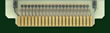
One final material you should know about is a selective plating for edge connectors or switch contacts. This is a Hard Gold Electro-Plate over Electrolytic Nickel underplate (Ni/Au), which is more durable than the Electroless Nickel Immersion Gold (ENIG) finish presented above. This plating will resist corrosion and its surface can handle the sliding/wiping action of contacts. The IPC recommends at least 0.8 um Gold (Au) over a minimum 2.5 um Nickel (Ni).
(Thanks to Happy Holden, for sharing his experience and his resources)
HowToPCB
Page One
Comments
Schematics
Terminology
THE END
Customers
Data
Tolerance
BEGIN
Material
Thermal
Trace&Space
Design
Place
Route
Check
CADtoCAM
QUALITY
HELP
Question
Organize
Who Me?