


Most aspects of Thermal Analysis are beyond the scope of this tutorial, but there's one topic you should know about:
Circuit Boards and Temperature
During assembly, components are placed into position and soldered at temperatures somewhere between 220 and 290 degrees C. The higher soldering temperatures are a result of new RoHS legislation (Restriction of Hazardous Substances) requiring solder to be lead free. Lead free solders require higher temperatures to reflow (~30C higher for Pb free), and this added thermal stress is a concern for circuit board reliability.
What happens to PCB material under thermal stress?
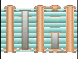
Most materials expand when heated, and the amount of expansion is expressed by a value called the Coefficient of Thermal Expansion (CTE). Copper has a CTE of 18, which means it expands 18 parts per million (ppm) for every degree C that it is heated. Epoxy resin, on the other hand, has a CTE between 30 and 40. This mismatch could cause problems if a PCB were to be manufactured with copper on a resin substrate. During thermal cycling, the difference in expansion rates would eventually cause de-lamination and/or solder joint failures.
The addition of woven glass cloth provides strength to the material, and constrains the expansion in the x-y directions to somewhere around CTE 17 (+/-2). This glass reinforcement brings the CTE of the substrate nearly equal to copper in the x-y directions, but the material under thermal stress must expand, so in the z-direction the CTE changes to somewhere around 70 (+/-20, depending on the type of material and ratio of glass to resin).
Looking at a material data sheet, you will always see the CTE(z), because it is the significant variable, but there is one more factor that makes the problem even worse. As a material heats up, it follows a fairly linear rate of expansion until it gets to the Glass Transition Temperature (Tg). At temperatures higher than Tg, the material expands at a different rate, sometimes approaching CTE 400!
It is the z-axis expansion and the higher rate of expansion above Tg that cause most of the problems related to thermal cycling.
This animation created by PWB, Inc. might help you visualize the bulging caused by thermal expansion:
Impact of Lead Free Soldering Temperature on Reliability
During electronic assembly, the circuit board and components must survive the soldering process, which is the highest temperature the product will ever experience. Adding to the effect of higher soldering temperatures is the effect of trapped moisture. Water Vapor pressure from trapped moisture is not linear, in fact it is nearly doubled with an increase of ~30C in soldering temperature. Moisture sensitivity and de-lamination is a greater concern than ever before.
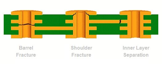
Thermal Load Driver 1 : Since resin is prevented from expanding in the x-y directions by glass reinforcement, and all of the 25C increase is ABOVE Tg, expansion in z-axis is much greater than in SnPb soldering, putting more stress on plated hole barrels (tension).
Thermal Load Driver 2 : Since drilling cuts glass fibers in the x-y direction, resin is free to expand near hole locations, putting stress on plated barrels trying to collapse it, much like a submarine in deep water (compression)
These stresses cause three types of failure related to plated through-holes:
Several other factors worth noting are:
- Thermal Degradation of the material at higher temperatures
- Resin recession from bulged hole walls (shrinks when cooling)
- Problems are worse on thicker boards than thin (<50mils)
- Materials cured with Dicyandiamide (dicy-cured) are economical but generally have less resistance to Conductive Anodic Filament (CAF)
Recommendations
- To reduce the higher expansion above Tg, choose a material with a higher Tg, at least 160C
- Choose a material that can stand up to the higher temperature without decomposing, a Td of at least 335C
- Require a de-lamination test such as T-288, 35 minutes minimum
- Choose a material with a more controlled z-axis expansion, maximum increase (from 50 to 260C) of 3.2%
- To increase resistance to CAF, choose a non-dicy-cured material
- Require greater plating thickness in hole wall, 1.2 mils minimum
- To improve hole wall plating, limit number of drill hits and resharpening
- Require GRADE 3 copper foil for internal layers, better properties
- Do NOT remove non-functional inner-layer pads, they add strength
- Restrict positive and negative etchback, both cause stress risers in the copper barrel walls
- Use the largest via diameters possible to reduce plating aspect ratio
- Require vendors to ship boards in moisture-proof packaging with desiccant and humidity indicator, and/or bake boards to remove moisture before assembly
- It is recommended for quality assurance and accelerated reliability testing to add test coupons to the fabrication panel for Interconnect Stress Testing (IST) and/or Highly Accelerated Thermal Shock (HATS)
Material Selection
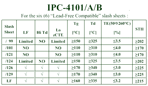
All circuit board materials are classified in the IPC document IPC-4101 (Specification for Base Materials for Rigid and Multi-Layer Boards). These materials are sorted into 55 "slash sheets" by type, and of these 55 slash sheets, only six are listed as Lead Free Compatible.
The problem is, currently only two of the sheets have characteristics that match the ones listed in the recommendations above! (/126 and /129)
Here is an IPC recommended fabrication drawing note for material:
MATERIAL:
LAMINATE GLASS FIBER EPOXY FLAME RETARDANT PER IPC-4101/126, 170C Tg MINIMUM,
DECOMPOSITION TEMPERATURE 340C MINIMUM, T288 DELAMINATION TIME 35 MINUTES MINIMUM,
MAXIMUM THICKNESS EXPANSION 3% FROM 50-260C.
PREPREG MATERIALS PER IPC-4101/126 SHALL MEET THE SAME REQUIREMENTS AS BASE MATERIAL.

(Thanks to Werner Engelmaier, for teaching us about reliability)
HowToPCB
Page One
Comments
Schematics
Terminology
THE END
Customers
Data
Tolerance
BEGIN
Material
Thermal
Trace&Space
Design
Place
Route
Check
CADtoCAM
QUALITY
HELP
Question
Organize
Who Me?