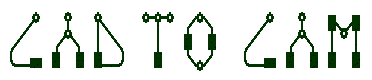
"Data May Not Be Modified..."
Sooner or later in the career of every circuit board designer, he will be called upon to leave the relative safety of his cubicle and venture out into the real world.
I've participated in about a dozen visits to circuit board manufacturing facilities, and each of those has included a brief stop in the CAM department. This is where the incoming design data is converted into the tools that will be used to manufacture the circuit board, including panelized artwork images and data for drilling, milling, test fixtures, inspection, etc.
In my experience, the discussion in this area has typically been something like this:
CAD: "Nice to meet you. Don't hesitate to contact us if you have questions or suggestions."
CAM: "Okay, thanks. No problems so far..."
And that's about the extent of the relationship.
(My attitude towards CAM? "No News is Good News!")
I know, I know, everyone says we should maintain good communication with our suppliers, but do we really need to contact them periodically? For no reason? What if we are competent designers and our designs are well within the current manufacturing limits? What should we discuss?

I recently had the opportunity to learn more about what happens to our data once we let go of it. I spent a day or two with Mike Tucker of P.D.Circuits to learn more about what the CAM department really does. (The P.D.Circuits CAM department is different than most. Instead of preparing data for a single manufacturing process, Mike is processing data for several different circuit board suppliers, so he has a fairly broad view.)
Although we've been hearing about the advantages of an intelligent data format for years, our company has always had good results with Gerber 274x, and we've never been confronted with a reason to change. When we are ready to order circuit boards, we send:
- Artwork layers (Gerber 274x format)
- Drilling Data and Drill tool table (ASCII)
- Fabrication Drawing (HPGL or PDF)
- Netlist (ASCII)
After our data passes through the Sales and Quoting department and into Front-End Engineering, Mike uses Frontline's Genesis 2000 to import it. (Other systems perform similar functions, but this article is not dependant on any particular brand of CAD or CAM software).
FRONT-END ENGINEERING
As circuit board designers, how many of you have a note on your drawing that says something like this:
"DATA MAY NOT BE MODIFIED WITHOUT WRITTEN APPROVAL"
Is it your intention that the circuit board supplier should make film from the data AS IS and run with it?
If not, do you have a clear idea what modifications are acceptable?
Let's imagine what our responsibilities would be if we were working in the CAM department. Our customers are using different software tools to do the circuit board layout, using different rules and parameters, and creating output data in different formats. We can't expect that any two of our customers will be doing the same thing the same way.
Our job will be to:
- accept data from many sources
- analyze the data and customer's requirements
- prove that they are acceptable to our process
- modify the data as needed
- output it to consistent formats,
- insert as a smoothly running stream into manufacturing
If we are doing a good job, we will never want to hear that manufacturing is having a problem using our data. ("No News is Good News", right?)
This is what happens:
Step 01 - Data Discovery
Since designers have a variety of naming conventions for files, most CAM systems have a feature that automatically examines the file internally to interpret the data type and format settings. The software's "best guess" is displayed on the screen.
Once they are identified correctly, the artwork layers and drilling data are often renamed or labeled for consistency or to aid subsequent processes.
If there are any missing files, files that won't load or obvious data errors, the job is put ON HOLD and the customer is notified.
Step 02 - Data Manipulation
Mike made sure all the artwork layers were aligned. Then he compared the drill data to the hole chart on the fabrication drawing, and separated the plated and unplated holes (they are used at different times in the board fabrication process).
Here is the raw drill data before sorting and editing

Any copper or silkscreen features that cross the board outline will be clipped to within 10 thousandths of the edge. Text or other drawn features outside the board edge will be removed.
If a netlist can be extracted from the CAD data, or if one is provided (preferably in IPC-D-356 format), it is compared to a netlist generated directly from the Gerber data, to look for discrepancies. If any mismatches are found, the job is placed ON HOLD and the customer is notified.
The following edits are made to improve the speed and accuracy of the Design Rule Checking (DRC) that will be performed in the next step:
- Arcs that have been created with a series of short segments are converted to a single smooth drawn arc
- Pads that have been created with draws are converted to flashes
- Planes that have been created with draws are converted to a single polygon contour
- Legend detection identifies text on conductive layers, so the checking process won't flag them as hanging traces
- SMD attributes detection identifies "pads without drills" to be understood as endpoints for netlist checking later
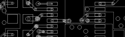
This is a view of drawn planes before contourizing
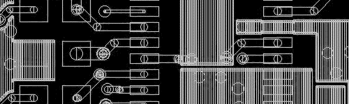
This is a view of the same area after contourizing. Any rule checking to plane edges will be much faster using the contour
At this point the netlist is verified again, to make sure any unintentional editing hasn't altered the design integrity.
Step 03 - Data Verification
During this phase, several different rules are used to check the design, to make sure variations in fabrication processes will still produce a reliable circuit board. These rules are typically set by default in the CAM system, but are often customized to meet the unique requirements of the customer. Here's what happened to my design:
- Minimums ? The minimum clearances and trace widths are identified. In our example, widths and clearances were collected and sorted into three categories; green, yellow and red. The green were okay of course, but the yellow instances were approaching limits, and the red items highlighted the need for cost/yield considerations and maybe even the need to put the job ON HOLD and consult with the customer.
- Profile check - Measure copper feature distance to board edge, contours, cutouts and unplated holes (10thou min)
- Drill diameters compared to copper pad sizes to make sure enough annular ring for minimum acceptability
- Possible slivers and/or acid traps are identified
- Stubs and hangers are located and reported back to the customer
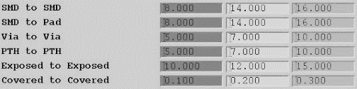
An example of rule settings using three levels of minimums for each attribute
Step 04 - Data Preparation
Final modifications are made to the data before it is sent out for fabrication
- Solder resist layers are examined to see if apertures have been expanded or supplied as 1:1 match with copper. Modifications here may shrink or expand mask as necessary and dam slivers may be removed, especially around fine-pitch SMT land patterns
- Silkscreen legend/nomenclature is clipped away from exposed copper (solderable) surfaces, using the soldermask edges as a boundary/cutting edge
- Non-functional pads may be removed, depending on the default practices of the supplier and/or the requirements of the customer
- Trace widths and/or dielectric spacing will be tuned to meet impedance requirements
- Compensation ? copper feature dimensions may be increased to compensate for etching processes
- Pad teardropping may be added to reduce drill breakout in "conductor to land" junction area
- Company logo/UL marking and date code added to design
Step 05 - Data Output
The data manipulation described in previous section was applied to the design as received, the steps listed below describe further manipulation to convert the design into production-ready tools. It would be difficult to list every possible variation, but every job will have a subset of these steps and have the same desired result (a working board the meets the customer's requirements for the highest yield at the cheapest cost).
- Individual or palletized designs (multiple boards placed in a single frame for ease of assembly) are arranged on the fabrication panel size (step and repeat)
- Etch Compensation - Layers may be stretched to compensate for fabrication process tolerances downstream
- Tooling features, thieving and tracking/identification added
- Routing data is created to excise the final product from the fabrication panel
- Files for final electrical test are generated
- Layers in the bottom half of the stackup are mirrored
The final task of Front-End Engineering is to output the final data into formats that are required by the specific fabricating equipment, and (if step-and repeat was performed on the CAM side instead of the CAD side) send paste screen and palletization data back to the customer.
Q & A
CAD:
As designers, we have been taught to define the data origin on a tooling hole if possible, but I never saw you use it for anything.
CAM:
Well, maybe the origin is useful to someone down the line, but not to us. What's more important is for all layers to have the SAME origin so they stack up correctly, including the drills.
CAD:
I noticed you didn't use the milling data we sent for routing the profile of the board. Why was that?
CAM:
We don't get that type of data very often. When we do, its usually not optimized for manufacturing and we have to modify it to minimize the tool path. It's a simple matter to create anyway, so don't waste your time trying to provide it for us.
CAD:
I noticed you changed the width of the features drawn on the silkscreen layers. Why was that?
CAM:
From our experience the customer doesn't care about the width specifically, he just wants it to be legible. Depending on the letter height, we adjust the width to work well in our process and give consistent results.
CAD:
When you receive a note stating "Data may not be modified without written approval", do you peform the CAM job any differently?
CAM:
Usually not. There are things we have to do to give you a good product, and the intention of the note does not pertain to those. Some customers are more than happy to have us fix things that we find as part of the service we provide, but others would rather fix it themselves and send new data. Either way is fine with us, and learning each customer's expectations is part of building a good relationship. Of course we rely on written communications in all situations.
CAD:
If you had one wish for improving the CAD-to-CAM process, what would it be?
CAM:
This is the only question that got multiple answers, which varied from "intelligent format" to "have every CAD operator spend a month in CAM, and every CAM operator spend a month on the shop floor" to "free ice-cream on Fridays"
RECOMMENDATIONS
Here are some ideas for making this process more efficient and less susceptible to error:
- Submit data in an intelligent format such as ODB++, but make sure your CAD system has implemented a reliable export capability. If you're not sure, send a test file to prove that your manufacturing partners can import it without difficulty. (you may want to create Gerber data in parallel as a backup for suppliers who can't import an intelligent format)
- Make sure the artwork layers and drilling files are created using the same format (If you don't know what to use, you probably can't go wrong specifying ABSOLUTE, NO ZERO SUPRESSION and either 2:6 for coordinates in inches or 3:3 if the units are in metric).
- Create a separate layer for the board outline, or plot it only for the soldermask layers. You don't want etched copper board outlines on every layer, or on the finished silkscreen
- Unless you really know what you are doing, generate paste mask openings 1:1 with the pad sizes. Unless the designer is known to have paid careful attention to expanding the paste mask apertures appropriately, the manufacturer would rather do it using a known starting place. Starting with mask that matches the pads makes the modification process much easier for the manufacturer.
- If you are okay with removing non-functional pads, leave them in the design so they can be used for drill/annular ring checking, and the CAM operator can remove them afterwards
- A unique aperture size used to draw planes, which is a different size than any of the thermal spoke widths, can be very helpful to CAM
- Make sure to differentiate which holes are plated and which are unplated
- If you are leaving it up to CAM to create an assembly array or pallet with breakaway tabs, make sure you leave spaces free of traces and components for the tabs
- ReadMe files are encouraged! Make sure to list any known netlist discrepancies
- Never try to perform your own etch compensation!
And finally, Preview your final output before you send it out!!! If you don't have a convenient way to do that, there are several FREE tools available, that you can find by searching the internet for GERBER VIEWER. If you can't download/install to your computer, here are two free online Gerber Viewers you might want to explore:
- http://www.circuitpeople.com
provides free online rendering based on their TrueGerber parsing and rendering technology. The site accepts single gerbers or zip archives of gerbers and creates PNG images which can be downloaded at resolutions from 25 to 600 dpi. Layers are loaded as thumbnails which are then viewed individually. If you choose to register with Circuitpeople, you will have the added ability to store designs and share a design through email - http://www.gerber-viewer.com
accepts single gerbers or zip archives of gerbers, accepts Excellon 1&2 format, can view multiple layers simultaneously with contrasting colors (good for comparing two layers), provides zoom and pan viewing, and printing with white background.
Both of these resources are free and don't require downloads, logins, or installation.
(Thanks to P.D.Circuits and Mike Tucker for investing the time)