


At this point you should have a general understanding
of
What a circuit board is
Who your customers are
and
What they need from you
Now let's go all the way back to the beginning, and start over.
Since no one does circuit board layouts on film with tape anymore, you will be using some type of software or Computer-Aided Design (CAD) system to get the job done. And what is the foundation of any CAD system? The Component Library.
Library work never seems to get the respect it deserves, but accuracy in mapping schematic symbols to appropriate component land patterns is the most essential core of any CAD system. One incorrect land pattern can lead to costly rework and revision across multiple designs.
SYMBOLS
We already looked at symbols in the section on SCHEMATICS, but what happens next is a procedure to interpret the schematic and:
- map its symbol pin numbers to component pin numbers,
- create a NETLIST of connections between them, and
- (if not done already) assign Reference Designators
This is called PACKAGING. The output from schematic packaging drives the PCB layout by providing a collection of component land patterns (logically identified by numbered Reference Designators) and the netlines that connect them together. From this data a Bill of Materials (BOM) can be generated, and the schematic SYMBOLS can be updated with Reference Designators and pin number assignments in a process called BACK ANNOTATION.
COMPONENTS
In order to create and maintain a library for your circuit board designs, you need to have a general understanding of electronic components. Here is a very brief overview of the major component families:
Leaded Components for Through-Hole Mounting
The early years of electronic circuits were accomplished using wires and sockets and components with metal tabs or round leads that could be bent into position and soldered. As circuit board technology advanced and the demand for mass production increased, most discrete wiring was replaced with etched circuit traces and component leads were inserted into plated metal holes and soldered on the other side. (This was the origin of labeling the top side of the board as the "component side" and the bottom as the "solder side"). Here are a few pictures:
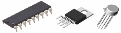
Through-hole components with only a few leads were generally fabricated with round wire, higher pin-count devices were fabricated with stamped metal frames which were subsequently bent into the desired shape, and many through-hole connectors were made with square posts or machined pins.
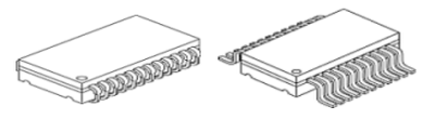
Surface Mount Components
Now imagine designing circuit boards for customers who want MORE components to fit in LESS space; the history of electronics has been driven by the desire to put more functionality into smaller containers. Let's look at one of the components pictured above, which is an integrated circuit with two rows of pins. This type of component is called a a "Dual-Inline Package", or "DIP". Using a 16-pin DIP on a circuit board requires a specific amount of board area on top of the board, and 16 plated holes going through the board. These 16 holes also use up space, not only on the surface layer but on the inner layers as well; space that could be used for routing more traces. Since we can't make significant gains by shrinking the pin diameter to reduce the plated hole size, what if we bent the pins outward or inward and soldered them to the SURFACE of the board? In this way we could save room by drilling much smaller holes only where needed for routing (this type of plated hole is called a "VIA"), and other surface mount components could be mounted on the opposite side of the board, increasing the circuit density. This idea had significant advantages, and manufacturer's started making components with surface mount leads instead of through-hole leads. Leads that were bent inward were called "J-leads", and leads that were bent outward were called "gull-wing" leads, because they resemble the wings of a bird.
As integrated circuit technology advanced, smaller and smaller die area was needed to perform equivalent functions, so surface mount component technology evolved into new families of components that were smaller, some of these were named "Small Outline Transistor" (SOT) and "Small Outline Integrated Circuits" (SOIC) series.
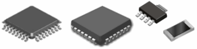
Discrete passive components like resistors and capacitors were fabricated in new form factors, rectangular "chip" components of various sizes with metallized end terminations.
Ball Grid Array (BGA) and Column Grid Array (CGA)
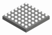
There are many different types of array components, and new packages with various styles, sizes and pin counts are being developed continuously. Some of the reasons for their popularity are:
- more connections can be placed into a smaller area, physical space requirements are reduced
- the leads are less fragile and the problem of bent leads is removed
- less material costs and packaging requirements result in cheaper products
- the distance between the active device and the termination is reduced, enabling faster signal speeds
Of course there are trade-offs that must be considered by using these packages, such as:
- denser packaging may result in greater thermal challenges
- solder joints underneath array packages are more difficult to inspect
- increased termination density may require additional board layers for trace routing
Bottom Terminated Components (BTCs)
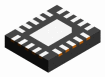
Some of the newer families of components can be grouped together based on one important characteristic, they don't have protruding leads. Their terminations are formed on the bottom of the component as flat solderable areas, in rows along two sides like Small Outline No-lead (SON) components, in rows along all four sides like Quad Flat No-Lean (QFN) components, or in multiple rows or arrays like Micro Lead-Frame or Land Grid Array (LGA) components. In addition to the circuit density advantages afforded by their small size and low height, and improved electrical and thermal performance, they are easier to manufacture which translates to lower component cost.
These advantages are partially offset by higher assembly costs, as these package types present a number of challenges:
- Bottom Terminated Components have no leads to absorb the stresses of thermal expansion/contraction
- Lower profile solder joints and less toe/heel/side fillet can affect long term solder joint reliability
- Lower stand-off height can be a cleaning issue if active flux becomes trapped underneath
- Marginal or missing solder joints are more difficult to inspect and rework
- Flatness in the circuit board (bow and twist) and final finish (planarity) will be more critical
The IPC has recently published the IPC-7093 Design and Assembly Process Implementation for Bottom Termination Components, containing information for users of these devices. In addition to design guidelines for circuit board layout, it identifies many of the characteristics that influence the implementation of reliable assembly processes and provides guidance information to component suppliers regarding ongoing issues.
Connectors
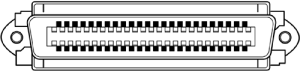
There is a wide variety of connector types with various body styles, termination counts, locking or latching features, current capabilities, mounting schemes, etc. Some are intended to mate once (or only a few times) during assembly and test, and may never be un-mated again during the life of the product. Others are designed to be used through-out the life of the product, requiring attention to human interface, access, safety, etc.
Any attempt to document the wide variety of connectors is beyond the scope of this tutorial, but what you need to know is how to incorporate all of these component types into board designs, which is the goal of the next section (Footprints and Land Patterns).
Component Summary
The ways in which electronic devices have been physically packaged are diverse, and they attempt to provide solutions for many different facets of the electronics industry. Some of these factors are:
- making reliable connections from the internal device to the external interface
- mechanically mounting the component to withstand the expected level of shock and vibration
- expected performance level over environmental variations like heat or humidity
- size and weight considerations using materials that balance cost with performance
- packaging in forms that aid assembly processes
We need to move on to the subject of CAD library footprints and land patterns, but there is a wealth of information available about components on the internet, both in a general sense and in specific detailed data sheets. You will be learning more about them for the rest of your career, but let me just point you to one more resource. There is a company called "TopLine" that makes dummy components for testing assemblies and assembly equipment, and they developed a tutorial that teaches about different component types and terminology, and contains more information than I could include here. So, with a big THANK YOU to TopLine, here is an excerpt of their "Dummy Class 101". (No, they aren't calling YOU a dummy, they are describing dummy component types). There's even a quiz at the end of each section to test your comprehension...
Okay, we're moving on to the subject of CAD libraries!
FOOTPRINTS AND LAND PATTERNS
At this stage of the electronics development process you should have enough attributes in your schematic symbols to package them into specific component types, or you will need some other source of data like a Bill of Materials (BOM) to perform this function. Schematics use similar symbols for a wide array of component types. Consider a capacitor symbol being used to specify a small decoupling device that can barely be seen by the naked eye, and the same capacitor symbol being used to identify a power storage device so large that it requires bolts to be mounted. At some point in the design process you must be able to identify the correct component for each symbol. You should be able to link each symbol to a specific component data sheet. I'm not implying that you should literally collect data sheets for every symbol, but the schematic symbols cannot be packaged into physical components without this information.
Once the required component types are known, we can proceed to the creation of the CAD library. Various types of components were described in the previous section, but they can be divided into two major categories; components that will be mounted into plated through-holes (PTH), and components that will be soldered to copper termination areas (called "lands") on the surface of the board. This second type is called Surface Mount Technology (SMT), but we will look at the design requirements for through-hole components first.
Through-Hole Components
Let's assume that our design will require a leaded LED device (Light-Emitting Diode), and that we have a physical description of it as shown here:
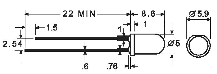
To mount this through-hole LED component on the circuit board, at a minimum we will need to provide two drilled holes spaced 2.54 mm apart (0.1 inch), and we will need to provide copper pads (at least on the back side) for soldering. For extremely inexpensive high-volume boards (without silkscreen or soldermask, and maybe even without plated holes) this may be all that is required. Cheap single-sided boards for many types of smoke detectors are designed this way, for example, but for more complex designs we will need to do more.
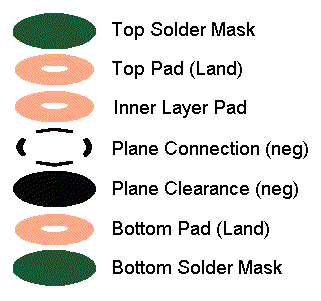
Modern multi-layer board designs will require:
- copper pads on both sides of the board,
- pads for any internal signal layer connections,
- openings in the soldermask so the pads aren't coated with "green stuff",
- openings in power planes that should not be connected to the leads, and
- a connection method if we want a lead to be connected to a power plane.
Each of these features needs to be sized appropriately for the diameter of the pin being used. In this example, the lead diameter for our LED component is 0.6 mm
Manually adding these features to the design would quickly become very tedious and error-prone, especially for designs requiring a large quantity of LEDs or components with more pins. Imagine trying to design a backplane with sixteen 180-pin through-hole connectors, or a design with many different component types with various pin spacings and lead diameters. Trying to add a feature to every layer for every pin would be impractical (not to mention the headache of trying to move a component), so CAD systems ncorporate the concept of "land patterns" and "padstacks" to make our lives easier. but before we can start working on those, we first need to know how to assign an appropriate hole size for each through-hole lead....
Determining the Hole Size for a Component Lead
To design a padstack for a specific lead diameter, the first question we have to address is "What size hole should we drill?". But before we can answer that question, we have to consider several factors related to tolerance. Although the concept of "tolerance" was introduced in a previous section, we need more information about hole diameter tolerances before we proceed.
If you aren't familiar with the concept of manufacturing Tolerance, you should read that section first and then come back here.
The plated hole sizes used for most components will need to have a diameter tolerance, typically +/-0.075 mm. The lead diameter of the component will also have a tolerance, but sometimes the lead diameter tolerance is not provided on the component data sheet. Regardless, we have to make sure that the largest lead diameter will fit into the smallest acceptable hole diameter, and still leave enough room for solder to flow into the barrel to make a reliable solder joint. The IPC recommends that the hole should be between 0.15 and 0.25 mm larger in IPC-7251 (Generic Requirements for Through-Hole Design and Land Pattern Standard) which hopefully will be published by the time you are reading this. Without this publication though, it is generally understood that the capillary action of molten solder flows best when the hole is 0.3-0.35 mm larger than the NOMINAL lead size, so you will probably be safe if you are using values close to these.
If your CAD system can maintain separate tolerances for each unique diameter of plated hole, its a common practice to list them in a hole chart on the fabrication drawing. For small holes used for through-hole component mounting (less than 2 mm), a tolerance of +/-0.075 mm is common, for large holes typically used for mechanical hardware (greater than 2 mm), a larger tolerance of something like +/-0.12 mm is typical. Holes for vias usually only require a maximum diameter tolerance. Since vias are only used to make electrical connections between layers, and nothing is to be insterted into them, the minimum size is not important. In fact, many designers allow vias to be plated completely closed (no diameter at all, a solid column of conductive material). Some designers are now moving towards specifying only the DRILLED diameter for vias (since often the drill size is more significant, especially in very dense designs) and don't specify the finished diameter at all.
Tighter tolerances can be maintained for unplated holes, because there is no plating variation to affect the finished diameter. I've seen tolerances similar to +0.05, -0.025 for unplated holes.
To summarize, the finished diameter of plated through-hole (PTH) can vary; typical values are in the range of plus or minus (+/-) 0.075 mm. This can increase to as much as +/- 0.012 mm for larger holes. The tolerance for unplated holes is typically +/- 0.05 mm unless the application requires more accuracy
Finally, although I've described some of these tolerances as "typical", don't over-specify without reason. For example, if your unplated holes can be +/- 0.075 with no adverse effects, you probably shouldn't specify a tighter tolerance. The parameters you list on your fabrication drawing will be inspected for quality and acceptability, so making the board more difficult to manufacture may affect yield and cost.
Keep in mind that you are specifying the FINISHED hole size; the fabricator will be using a larger diameter drill size to make enough room for the plated hole walls. It may help to know that there are standard drill bit sizes, you can refer to this DRILL CHART if you want to know more about that.
Now, to get back to our example of a through-hole LED with 0.6 mm lead diameters, we are going to use a 0.8 mm hole size with a tolerance of +/- 0.075 mm
Padstacks
Most CAD systems work in a similar way when creating and storing padstacks. Simply put, a padstack is a set of shapes designed for a specific plated-hole diameter. A unique padstack will be created for each hole size used in the design. A simple example is shown here:
to be continued...
Finally, you should know that for most through-hole parts, PIN 1 is identified by using a square pad on the surface layers instead of a circular one. In many cases this makes it easier for the assemblers to see the proper component orientation, so they can insert the component into the bare board correctly, even if there is no silkscreen or other polarity marks.
Tom Hausherr has created a proportional set of padstacks for all common through-hole lead sizes that he is willing to SHARE, (and more information related to a universal PCB CAD Library will soon be hosted by him at PCBpod.com)
Land Pattern "Extras"
After assigning padstack information to each component lead (and mounting, if applicable), other features may be added to the overall pattern. Silkscreen (epoxy ink) can show the polarity of the component, the Reference Designator, and often an outline of the part as a visual reference. Specific areas of the soldermask layer may need to be cleared away for access to heat-sinking features.
Other non-visible attributes may be added such as a component origin for placement/rotation or a courtyard boundary to ensure a minimum clearance to other components.
Surface Mount Components
to be continued...
A very good series of articles about CAD library structures was written by Tom Hausherr
and published by
PCBDESIGN007.
If that link doesn't work, try HERE.

FILE NAMING CONVENTION
I also want to mention the importance of developing a good file naming convention. The way you name the elements in your CAD system will become increasingly more important as your system grows and becomes more complex.
Hopefully you will never need to:
- open a file to make measurements because you can't tell what it is from its name
- make a duplicate file because you can't find the existing one you need
Your library will eventually become one of your most valuable assets and will represent a considerable investment in time and effort. The method you use to name files should be considered for all aspects of your CAD system; components, symbols, padstacks, design names, etc., and should be flexible enough to incorporate new technological developments. After you gain experience you may wish you could start over using a different convention. Many of us have faced this task over and over again as new CAD systems are developed and new tools are adopted.
(Thanks to Tom Hausherr, for systemizing and standardizing)
HowToPCB
Page One
Comments
Schematics
Terminology
THE END
Customers
Data
Tolerance
BEGIN
Material
Thermal
Trace&Space
Design
Place
Route
Check
CADtoCAM
QUALITY
HELP
Question
Organize
Who Me?