We need to have a clear goal in mind.
What exactly does a circuit board designer create?
What is expected of us?
So... We are starting at the END.
Your goal as a circuit board designer
is to convert ideas into reality.
A schematic is a way to describe someone's idea by using symbols that anyone who knows electronics can understand. But it's still just an idea. The schematic must be converted into something physical that can be manufactured and tested.
What is a Circuit Board?
A circuit board provides a substrate to mount electronic components on, and provides conductive connections between them. It is constructed with layers of conductive material (usually copper) separated by layers of insulating material (usually a flame-retardant epoxy reinforced with glass fibers). The board not only connects everything together, it also provides mechanical support for the components.
Electronic components must provide a way of
making electrical connection to the board.
Sometimes these connection points take the form of wire leads (like many connectors, axial capacitors or radial resistors, for example), sometimes they are part of a metal frame that is stamped and bent to provide electrical connections (like DIPs, gull-wing or J-leaded devices), sometimes they have metal spheres, posts or columns (usually these are area-array devices like BGAs), and some provide only planar conductive termination areas (referred to as "leadless" devices, like QFNs or BTCs).
Regardless of the type of conductive terminations employed by the device, the circuit board must provide a plated holes or conductive land patterns to make the connections to the component. After the device is placed on the land pattern, it is welded in place with a material called SOLDER that is also conductive.
Soldering components onto a circuit board accomplishes two things:
- it provides the mechanical attachment that supports the component, and
- it provides an electrical connection between the component and the board.
The printed board has etched conductors on one or both sides (and may contain additional inner layers of conductive circuitry) to connect the plated holes and land patterns together.
Conductive lines that connect land patterns together are called TRACES, larger conductive areas are called PLANES, (also commonly referred to as COPPER POURS or AREA FILLS), and a Plated-Through Hole (PTH) that connects layers together is called a VIA
This simple illustration highlights the major features of a circuit board
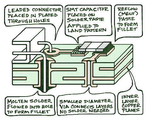
This is a four-layer board, which means it has four layers of conductive copper; one on top, one on bottom, and two inner layers. The two inner layers are planes (one for power and the other for ground) The connector leads are inserted into plated-through holes and soldered from below, but the surface mount capacitor is placed on a layer of solder-paste (applied to the lands before component placement, as shown on the left end of the SMT cap) and heated until it melts, forming a solder fillet between the component termination and the land (shown on the right end of the component). A via is shown connecting one end of the cap to an inner plane.
This is a photograph of an actual circuit board. You can see three SMT land patterns and some test points, with traces / vias connecting them together.
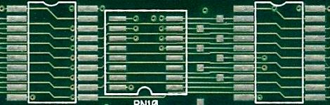
There are three other important things to notice in this picture:
- Green soldermask has been applied to the surface of the board, leaving openings in areas that will be soldered and for test point accessibility.
- White silkscreen provides identification of parts by reference designator and component outline
- A final finish has been applied as a protective coating over exposed copper, keeping it solderable. In this example it is an alloy of Tin and Lead (eutectic solder), but it could also have been silver, gold, tin, or an organic solder preservative (OSP)
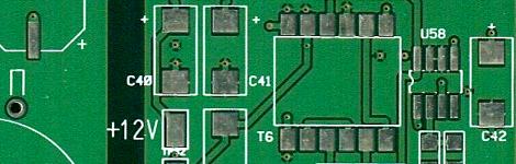
Here is another example, but it shows some AREA FILLS, sometimes called copper POURS. Also notice that the silkscreen can be used to provide extra nomenclature, like the "+12V" label, which may help people in the lab or during field service. Try to consider the needs of others who may be using your product long after you have moved on.
To summarize,
Creating a board shape that fits the physical size requirements,
positioning the mounting and tooling features,
determining the number of routing layers (cost vs. performance),
logically arranging circuits into functional areas (floor-planning),
populating each area with appropriate land patterns (placement),
adding planes&traces to connect everything together (routing),
and generating data to fabricate, assemble and test the product
is what circuit board designers do.

(Thanks to Pete Waddell and his PCB Design Conferences)
HowToPCB
Page One
Comments
Schematics
Terminology
THE END
Customers
Data
Tolerance
BEGIN
Material
Thermal
Trace&Space
Design
Place
Route
Check
CADtoCAM
QUALITY
HELP
Question
Organize
Who Me?