At this point we have:
- packaged the schematic, which mapped all of the symbols into corresponding components and assigned unique reference designators to them, and
- entered some kind of board outline or boundary which defines the area we can use for component placement.
Depending on the CAD system, your layout environment may look like a jumble of components with a ratsnest of netlines connecting them all together, or it may be completely empty, waiting for you to select parts one at a time (or in groups) for placement.
It would be very difficult to mentally keep track of everything we need to remember for a complex design, so we depend on the computer to maintain connectivity and help us keep track of any built-in rules. Even with computers helping us, looking at perhaps hundreds or thousands of parts that need to be placed intelligently can be very intimidating;
How Do We Start?
We can develop a "plan of attack" by logically breaking down the final goal into smaller steps. Some of the steps can be accomplished immediately and you probably won't have to worry about them again (like placing mounting holes). Others must be maintained throughout the design process (like component height restrictions). These should either be incorporated into the CAD system by creating design constraints or rules, or added to a manual checklist for the review process to make sure the design meets all expectations.
(USE THE CAPABILITIES OF YOUR CAD SYSTEM!)
MECHANICAL CONSTRAINTS
Component placement will be confined to a limited area, which may have to be reduced even more by mounting considerations. Before you start placing parts, make sure any mounting holes have been placed at the proper locations and that you know how much clearance area is needed around them. If your CAD system supports it, lock these down in a way that prevents you from accidentally moving them.
Depending on the final assembly, there may also be clearances needed for tooling, card ejectors, brackets, etc. as well as component keep-out areas and areas with component height restrictions. Some CAD systems provide a way to define these "keepout" areas so the computer can report violations during automatic checking, others prevent violations from occuring at all.
Next, there may be components that have pre-defined locations. Depending on the next-level assembly, connectors might have to be placed with a specific orientation to mate with other parts of the system. Switches, displays, indicators, LEDs, variable components and some types of test points may need to be placed for accessibility.
Place all of the components with pre-defined locations first.
ASSEMBLY CONSIDERATIONS
It will help to know how your board will be assembled and tested. Will the bare boards be processed individually or in arrays? If individually, will the boards need extra rails for support? If palletized in arrays, how will they be separated? Will you need clearance for v-scoring? routing? tab-cutting? Can your design have parts on both sides? If there are through-hole parts, will they be wave soldered or selective soldered or hand soldered? Will an In-Circuit Test (ICT) fixture be developed? Don't panic, these questions aren't being asked to make your job more difficult. You may not know all of the answers, but component placement can influence assembly processes later on, and knowing something about them may help you design a better product.
If your design will be built using an automated assembly line, you may need to add fiducials and extra tooling holes, which will use up more of the board area. Get these placed before you run out of room.
If the assembly will be transported from place to place using conveyors, you will need to keep components away from the edges. If your design is small and will be assembled in a pallet array, the pallet itself will provide rails that are discarded later. In this scenario you may be able to use the full area of the board for placement, leaving only enough clearance for singulation tools (breaking the boards apart at the end). Otherwise, you will not be able to place components too close to the board edge.
If the boards will be assembled individually, keep components 3mm away from the board edge.
You will decide which of several placement schemes will work best for your design, which will define a specific assembly TYPE. The type that you choose will determine the basic steps required to assemble the product.
If you can fit all of the parts on one side of the board you probably should. One-sided assemblies are designated as TYPE 1:
TYPE 1A - All Through-Hole parts.
	  The easiest type to assemble and solder
          manually, automatic component insertion
          is more difficult than TYPE 1B, but can
          be wave-soldered with a single pass.
TYPE 1B - All Surface Mount parts. Assembled using
          a single paste screen and a single pass
          through component insertion and reflow
          soldering. IDEAL.
TYPE 1C - Mixed assembly SMT and Through Hole, two
          soldering passes required.
If you have to place components on both sides of the board, it automatically becomes a TYPE 2 assembly and will require a greater number of assembly processes.
TYPE 2A - Through-Hole parts on both sides.
	  requires manual processes. NOT RECOMMENDED.
TYPE 2B - Surface Mount on both sides.
	  (Try to keep active devices on same side)
TYPE 2C - Complex Intermixed assembly on both sides
You should have an idea of the assembly type that is most appropriate for your design before you start placing components. Limited placement area (circuit density) may drive you towards using both sides of the board, and the component types required may drive extra assembly processes that can influence placement.
Before proceeding, determine if your design will be a one-sided or two-sided assembly
SOLDERING
If through-hole components are inserted from the top, they will usually be soldered from the bottom using Wave Soldering or Selective Soldering.
Wave Soldering
This method moves the bottom of the board over a molten wave of solder, and when the wave touches any exposed metal it will be coated. Where two exposed metal surfaces are touching each other (like a lead in a hole or an SMT termination sits on a land), a solder joint will be formed between them. Surface Mount devices are often attached to the bottom of the board with adhesive and then wave soldered.
What does this have to do with component placement?
If the design will be wave soldered, parts should be aligned or oriented to the direction of wave to prevent solder shorts or open connections. For example, if you put a very small component behind a very tall component, as the wave passes over the tall component it could create a "shadowing effect" which may result in the smaller component having insufficient solder or none at all.
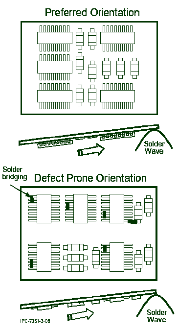
This illustration shows how surface mount parts should be rotated with respect to the wave direction:
Selective Soldering
If there are only a few through-hole connections that need to be soldered, assemblers may choose to do selective soldering for just those through-hole leads, and reflow solder the rest. If selective soldering will be used, maintain a 6mm diameter keepout area around each through-hole.
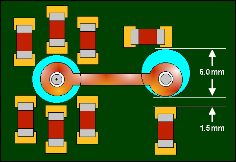
If passives must be placed closer to the through-hole pin, the selective soldering nozzle can be offset, but make sure there is enough room on the other side for the full 6 mm clearance diameter, and make sure there is at least 1.5 mm from pad to pad. Also, if the selective solder nozzle heats both ends of a passive SMT device at the same time and they both reflow, the component may fall off the board. Try to place passives "in-line" (one end close, the other farther away).
TESTABILITY
One more consideration before we get started placing parts - If an In-Circuit Test (ICT) fixture will be required, you will have to add extra vias for test point accessibility to every net. Since the goal is 100% accessibility to every net from the bottom of the board (double-sided fixtures are more expensive), even short traces that can be routed on the top of the board have to use a via to get to the bottom-side for a test point. Adding vias to every net means extra space between components, so keep this in mind (or just add them) while you are placing functional groups of components.
COMPONENT PLACEMENT
Ok, that was a lot of preparation...
At this point you should have mounting holes, tooling holes and fiducials placed, keepout areas defined, and components with fixed locations placed and locked down. You've decided whether your design will have be single-sided or have parts on both sides.
Now, let's get started placing components!
EMC
It is generally a good idea to keep I/O lines interacting with the outside world away from internal signals. Most schematics with connectors also have some kind of passives (ferrite beads or caps or transorbs) that should be placed near the connector pins, and the traces connecting them should be relatively short to reduce the amount of noise coming in from the outside world.
Since we already have our connectors placed, it might be a good idea to go ahead and place the passives related to each node.
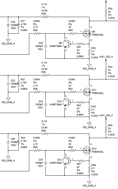
Here is a simple example of some passives that need to be close to the connector pin:
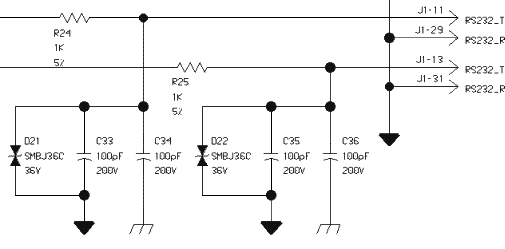
All components that touch the node connected to J1-13 should be placed close to J1-13 to keep that node area confined. This picture shows one way of doing it for a single sided assembly:
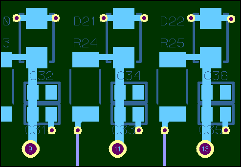
Components on the other side of R24 and R25 (not shown) can be placed elsewhere. Continue placing components tied to connector pins until all I/O lines are done.
FLOOR PLANNING
Now its time to take a step back and look at the big picture. Since there are so many different types of board designs, it would be difficult to make specific statements about how you should proceed. But in a broader sense, electronic circuitry has some kind of flow, input and power comes in from somewhere, something happens to the input internally, and some kind of result goes out.
Regardless of how the circuits are placed on the schematic pages, the floor-plan of the design should be somewhat logical. We want to keep functional groups of circuitry together, we don't want groups interfering with each other, and we don't want critical signals crossing back and forth over each other. Analog circuits should be separated from digital circuits. High frequency circuits should be isolated from low frequency circuits.
Try to get a mental picture of the best way to place the functional groups of components so the circuit flows logically.
If the design is very complex and you aren't sure how it should fit together, you can start working on the functional groups individually, and then shuffle the groups around later to make them fit together.
FUNCTIONAL GROUPS
Here is the general approach I use for almost every design I do; After performing the steps that have already been described, I:
- scan through the schematic, mentally taking note of groups of components that look like they belong together, like four op-amps that are packaged into the same IC.
- look for circuits that aren't anything like the rest, for example there may a power supply that has high current requirements and very large components, where everything else is smaller. One single circuit like this with special requirements probably needs to be done first using specific rules, and then moved into location in a particular area of the board, like near a power connector. If I see anything like this I will probably do it first and put it where it belongs on the board.
- keep routing in mind. Although the focus of this tutorial is on placement, routing considerations can heavily influence placement decisions. If the design is primarliy large digital devices, they will be arranged to optimize performance of clocks and r buses (and possibly timing delays).
- pay particular attention to repetitive chunks of circuitry, for example there may be twelve channels of identical circuitry for a particular design. In this case I would do one "perfect" channel placement, taking extra time to massage the overall shape of the group into a rectangular arrangement, or some shape that will allow me to place the other eleven channels without wasting too much board space, and then copy the remaining channels to match
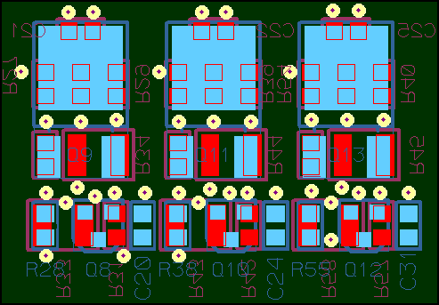
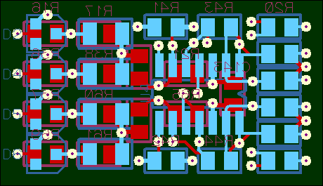
Here's an example of duplicate circuitry:
and how I would place them as identical blocks on a 2-sided assembly. The top-side components are blue, and the bottom are red. I added short traces and vias to make sure the blocks would route, but removed them in the picture so you could see the components more clearly.
For more complicated functional groups, I generally place decoupling caps first, then higher frequency components like crystal oscillators and associated circuitry (which might be considered more important than decoupling, but they rarely interfere with each other), then feedback components or components in the "critical path", and then all the miscellaneous passives like pull-up or pull-down resistors. As I go, I make sure to leave room for via fanout, quite often putting them in as I go. In fact, I usually do the very short routes from pin to pin WITHIN the group on surface layers, and then all the routing BETWEEN groups will be done on INNER layers after the groups have been shuffled into their final positions. If you use this method, make sure you add test point vias if ICT will be required.
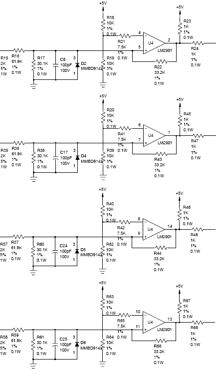
Here is one more functional block:
As you place components, leave at least 2.5mm between ICs for visual inspection of solder joints and possible rework, and keep at least 1mm space between passive component bodies (land pattern edge-to-edge spacing may be less).
OK, that's enough examples. Keep sorting out groups until you have all your blocks done, or enough to start organizing them on the floor plan.
Even if large active devices don't seem to have an obvious group (or are connected to too many devices to manage easily), at least place all the required decoupling caps and other passives like pull-up and pull-down resistors. I usually try to put these underneath the large ICs so I can move and rotate them in convenient chunks.
When you have most of the groups sorted out, zoom back out to see the big picture again. You have functional blocks of circuitry placed, and now its time to to arrange them in some logical order. If you have been following the method outlined above, most of the short routes within the blocks are done, most of the fanout vias are in, and now it may be easier to see the netlines connecting the blocks together.
POWER DISTRIBUTION
Even though you have made good progress on organizing components into groups, the remaining netlines may still look very complicated, and another way to help sort out the floor plan placement is often clarified by looking at the power requirements.
For example, many modern circuit board designs have several different voltage levels used by various sections. If there are many different voltages it will be impractical to devote entire planes to each one, so you may have to fit several voltages on a single layer by using split planes. Most of the time you will want to keep blocks using similar voltages together for the most efficient power distribution.
If your CAD system allows changing colors by net name or net type, try setting all nets to a dim neutral color, and then set each voltage level to a different bright color. By looking at the design in this way, you can sort out the blocks for different voltage levels quite easily. Quite often you might have a predominant voltage for the majority of the design (like 5V or 3.3V) and then miscellaneous smaller areas of other power requirements like +/-12V or 2.5V or 1.2V, etc.
I usually group the smaller voltage areas together first, with any associated voltage regulators and bulk capacitance, and place them in a way that flows from one to the next. For example, a 12V power supply will feed any 12V circuits (so you will want to place them close by), but also provide the input to a +5V regulator, and then the +5V plane might supply power for a large amount of circuitry, but also provides the input for another regulator that drops down to 3.3V for that section. Try to place these cascading sections logically, and keep the routes for each section confined to that section as much as possible, without crossing over plane splits.
FINAL WORD
Without knowing the particular characteristics of your design, it is difficult to say more about how you should proceed. Every design is different, and a strategy that worked well on one design may give poor results on the next. Learn from similar designs if possible. If the schedule allows, take a challenging circuit and try a few different approaches. You will get better and better at it the more you practice. Be alert to circuits that have been copied from previous designs; look back to see how it was solved before and either improve on it, or think about saving it in a way that can be reused in the future to save time.
When all of the components are placed, review your original rules (like height restrictions or keep-out areas) to make sure nothing was overlooked. You may also want to host a placement review before the final routing phase begins.

(Thanks to schedulers and supervisors who allow enough time to "Do It Right The First Time")