


Over the years, we have developed ways to control the flow of electricity for many useful purposes. These techniques can be recorded and shared by using diagrams called schematics. A schematic diagram is a convenient and informative method for documenting electronic circuitry.
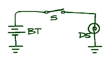
Anyone who understands basic electronic theory can explain the following schematic, no matter what language he speaks.
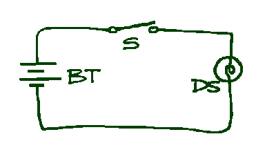
The basic building blocks of schematic diagrams use a set of standardized symbols to represent different component types. In the schematic shown above, the symbol next to the BT represents a battery, the symbol next to the S represents a switch, and the one next to DS represents a display or a lamp. The letters BT, S, and DS are labels that help identify the component, and these labels are called REFERENCE DESIGNATORS.
Anyone who knows how to interpret the schematic can build the circuit it represents by connecting a battery, a switch and a lamp together with wire or any other form of conductive material.
SCHEMATIC DIAGRAM - A drawing that shows, by means of graphic symbols, the electrical connections, components, and functions of a specific circuit arrangement

Symbols and Reference Designators
These are the most common symbols you will see on schematics,
and the Reference Designators that are used to identify them.
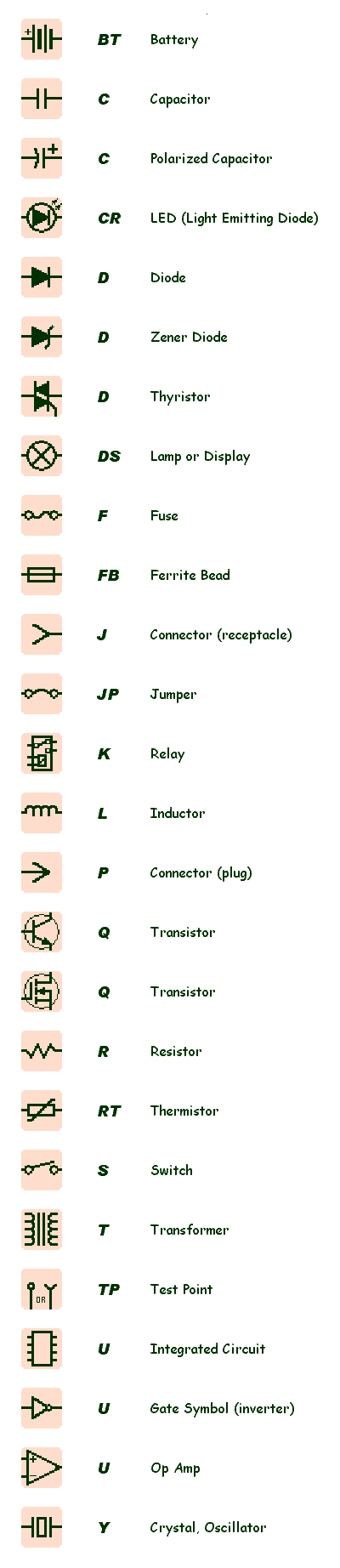
For you trivia fans, the origin of the reference
designator "U" meant "Unrepairable".
Note that some Reference Designators are used for more than one symbol. Even though there are separate symbols for "capacitors" and "polarized capacitors", the reference designator for both of them is C.
Integrated Circuits, Modules (like power supplies) and Sub Assemblies (like daughter boards) are usually drawn as a rectangle with a number of pins attached. Thousands of components share this symbol style and the U reference designator. Many components have so many pins that the symbol has to be divided into multiple parts.
In addition to Reference Designators, symbols are also assigned numbers to differentiate components of the same type. For example, if more than one resistor is added to a schematic, they will be labeled R1, R2, R3, etc.
This is not a complete set of symbols, but it should be enough to get you started. For example, there are many types of transistors, but only two are shown here. As a circuit board designer you probably won't have to know the difference between them. For now, you just want to get a general idea of what they look like.
When you are ready to learn more, a more complete list of symbols and reference designators can be found in the publications
IEEE STD 315 and IPC-2612
Values and Attributes
In the example schematic above, there is not enough information to know what is intended. The components are identified by a reference designator (the letters BT, S and DS), but there is no information about what type or what size the components should be. Consider the fact that there are many different types of batteries available, but nothing in the schematic above suggests which battery would be best. The circuit shown above could be:
- a simple flashlight with a size AA battery, or
- a 9V battery, a doorbell button and a buzzer, or
- a 12V car battery, a rotary switch and a headlamp.
Applying the same basic circuit to these different applications illustrates the fact that in the real world, a schematic must provide more information. A schematic must include ATTRIBUTES to insure that appropriate components are selected. The same resistor symbol can be used for thousands of different kinds of resistors, so to be useful it must declare the VALUE, expressed in ohms. The ohm symbol is usually dropped because it is not available in all character sets, so a resistor with the number 100 next to it would be interpreted as "a hundred ohm resistor". Other types of components are described with different terms; capacitors are differentiated by their value in farads (F), inductors are differentiated by their value in Henrys (H)
Many additional attributes can be added to symbols (Power Ratings, Tolerances, etc) to more tightly control the type of component needed for the design.
In addition to visible attributes for each symbol, many Computer-Aided Design (CAD) systems can also assign hidden attributes such as manufacturer part numbers, cost, revision levels or simulation data. Although a discussion of various CAD capabilities is beyond the scope of this tutorial, sophisticated libraries can be developed with them, and schematics created from them can become very powerful tools.
International System of Units (SI)
Attributes can have a wide range of values, from very small to extremely large. To avoid filling diagrams with long repeating strings of zeros for values like 1,000,000,000 or .0000000001, the world has converged on an International System of Units.
The SI units you are likely to see on schematics are:
| SI UNITS | ||
| PREFIX | SYMBOL | VALUE |
| tera | T | 1 000 000 000 000 |
| giga | G | 1 000 000 000 |
| mega | M | 1 000 000 |
| kilo | k | 1 000 |
| (none) | 1 | |
| milli | m | .001 |
| micro | u | .000 001 |
| nano | n | .000 000 001 |
| pico | p | .000 000 000 001 |
Some examples:
- a .000027 Farad capacitor would be expressed as 27 microFarads, written as 27 uF
- a .05 Henry inductor would be expressed as 50 milliHenrys, written as 50 mH
- a 10,000,000 Ohm resistor would be expressed as 10 megaOhms, written as
10 M
(not all computers/CAD systems supported the ohm symbol, so it is usually not used)
Notes:
- SI declares that there is a "no break" space between the number and the symbols, but many CAD systems do not follow the standard, so you will see it both ways, i.e. 10 uF or 10uF
- Symbols are not pluralized. For example, 10uF should never be written as 10uFs
- Symbol names are written in lowercase unless they are based on a person, like the Pa unit of pressure (called a Pascal).
- Symbols are written in lowercase unless they are greater than 1000 (kilo)
More about SI Units
You can get more information about the International System of Units (SI) from the National Institute of Standards and Technology (NIST). They maintain very good website at http://physics.nist.gov/cuu/Units and the document that describes SI in detail can be found in the Bibliography (online publications and citations) as Special Publication 811
Symbols, continued...
There is one more category of symbols you need to know about, symbols that don't have reference designators. These symbols don't represent components, they represent electrical connections.
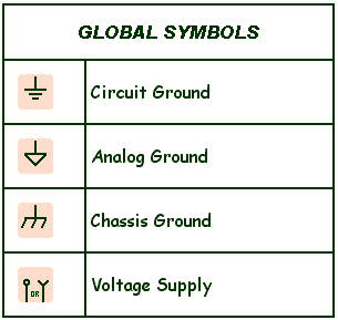
In a complex circuit, if every power and ground net were shown connected together with lines, the diagram would be too cluttered, and more difficult to interpret. Instead of showing them connected with lines, we use GLOBAL SYMBOLS. Anything connected with the same global symbol, even across multiple sheets, is assumed to be connected together.
The circuit below is equivalent to the one shown previously:
The Ground Symbols in this simple circuit don't help the readability very much, but replacing the clutter of numerous power and ground lines in a more complex design is a usually good practice.
Schematic Design Guidelines
- Lines connecting symbols together represent electrical connections between components. Lines that cross each other are NOT connected.
- A CONNECTION DOT is used to show connections between lines that touch, but it is better not to have four wires that connect at a point (don't have lines that cross and connect). In other words, a connection dot will typically have three line segments attached to it
- In a complex circuit, if every power and ground net were shown connected together with lines, the diagram would be too cluttered, and more difficult to interpret. Instead of showing them connected with lines, we use GLOBAL SYMBOLS. Anything connected with the same global symbol, even across multiple sheets, is assumed to be connected together.
- If other connections need to be made without connecting lines together (across multiple sheets, for example) NET NAMES can be used. Any net labeled with the same net name is connected.
- All text (pin numbers, net names, polarity, values and attributes) should be horizontal and clearly labeled to avoid confusion. NO OVERLAPPING TEXT, NO LINES CROSSING THROUGH TEXT.
- Circuits should flow from left to right and top to bottom. What this means is, try to keep inputs on the left and outputs on the right, and try to keep positive voltage supplies above and ground symbols below.
- Try to design schematic sections in functional blocks. Symbols are placed on the page to facilitate an understanding of the circuit, not to show where they are physically located on the board or to show which connections should be long or short.
- Don't try to fill the whole sheet, and don't be afraid to leave empty areas or open spaces.
- Align similar circuit symbols vertically or horizontally. You might not have time to make everything as beautiful as you wish, but schematics should be easy to read and unambiguous. It may be helpful to use a grid if your CAD tool supports it.
- Pin numbers should be on the outside of the symbol graphic. Net names can be placed inside the graphic if practical.
- If sheet connection symbols are used, they should be placed on the extreme left edge or extreme right edge of the page.
- Depending on the conventions of the company or customer, you may have to provide additional information such as an IC Power Table, or a list of spare gates. These are often placed on the last sheet.
- The first sheet should contain a title block in the lower right corner. At minimum it should contain the Part number, Title, Revision Level and the name of the person who created it. Titles should be distinctive enough to differentiate the design from other similar designs. (You don't want to end up with dozens of designs named "Amplifier", for example). Subsequent sheets may have a reduced title block, but must contain a sheet number and some method of identifying it as belonging to the design (at least the part number and revision level)
The process of entering a schematic into circuit board development software (CAD tools) is most commonly referred to as SCHEMATIC CAPTURE.
This is a typical example of what schematics look like:
Each CAD system has a different set of features, and common features among different tool sets are often implemented in different ways. When using computer software to perform schematic capture, you should take advantage of the capabilities the CAD tool provides. (Maybe I should stress that point more boldly...)
Learn the capabilities of the CAD tools you have access to!
For example, most CAD libraries will already have the Reference Designator assigned to the symbol (R for resistor, L for Inductor, etc), and during the process of packaging the schematic symbols into actual components, the software will number the instances (C1, C2, C3, etc) and update the schematic automatically. So, in most cases, you don't have to take the time to manually assign reference designators. Let the computer do the work, unless you have a reason for specifying it. In some cases you may want a particular connector to be named to match existing documentation or another assembly, or you may want specific op-amps to be packaged together into the same IC. In these cases you may need to assign the Reference Designators yourself.
Another benefit of most CAD tools is the ability to declare NET ATTRIBUTES. If the design contains a net that must carry 5amps continually, and your CAD tool supports the ability to add a "5amp" net attribute you should make an effort to declare it, where it will be retained permanently. Building intelligence into the design at the schematic level will streamline subsequent design processes, saving time and reducing the chance for error or oversight.
Each CAD system has a different set of features, and common features among different tool sets are often implemented in different ways.
Design for Manufacturability (DFM)
DFM is a topic that touches on every aspect of circuit board development. One subset of DFM is Design For Test, or DFT. Many products will be tested after assembly (component placement and soldering) to make sure everything is connected together properly, and without unintended connections (shorts). One of the ways this is done is by using an In-Circuit Test fixture (ICT).
The details of ICT fixture and program development is beyond the scope of this tutorial, but there are several things you can do at the schematic capture level to improve testability. If ICT will be used on your product, you should:
- Tie IC control lines high or low using individual pull-up or pull-down resistors
- Tie unused inputs high or low using individual pull-up or pull-down resistors
- Include method to disable clocks (can be accomplished using jumpers, tri-state buffer or enable line of oscillator if available)
- Provide disable methods for Programmable Logic Devices (PLDs), Application Specific Integrated Circuits (ASICs) and other custom devices
- Provide disable methods for Bussed Devices, High Current Devices, Flash RAMs, EEPROMS and D/A Converters
- Provide circuitry to disable digital feedback loops
- Provide a means to disable On-Board PROM
- Isolate Power-On Reset circuits from other digital circuits
The schematic provides enough information to select appropriate components and connect them together during the circuit board design phase. Schematics also provide a basic level of documentation for electronic products, and become useful tools during design reviews, testing and debugging, field service, technical manuals, etc.
That's as much as we need to know about schematics for now.
!!! YOU MUST READ THIS !!!
VERY IMPORTANT FINAL NOTE
None of this is set in stone, and every company or customer has slightly different preferences. I have never seen two companies do things the same way. Take what you see here as a place to start, but try to learn their particular style as quickly as you can.
The first thing you should do is study some of their existing drawings. Some companies use "D" as the reference designator for LEDs, others use "LED". Some use a little circle for test points, some use that same symbol for voltages. Some use a rotated connector symbol for voltages. It doesn't really matter as long as it is clear and consistent. After you build up some experience you can suggest ways to standardize if you think it will help.
Go with the flow,
and don't make waves 'til you know what yer doin'.
And by the way, if you move to a NEW company and they do everything differently, don't bother saying "Well, at my last company we did it this way". Chances are, they won't care.
(Thanks to the U.S.Navy and Devry Institute of Technology for teaching me the basics)
HowToPCB
Page One
Comments
Schematics
Terminology
THE END
Customers
Data
Tolerance
BEGIN
Material
Thermal
Trace&Space
Design
Place
Route
Check
CADtoCAM
QUALITY
HELP
Question
Organize
Who Me?
If you don't know much about electronics, these may help you get started.
Books specific to circuit board design will be presented later...